Texas Instruments CDCR81 Direct Rambus Clock Generator Data Sheet
Summary
The CDC921 Direct Rambus Clock Generator provides essential clock signals required for optimal operation of a Direct Rambus memory subsystem. This manual offers comprehensive instructions on utilizing the device's advanced features, including phase-locked loop (PLL) controlled synchronization, multiple operating modes (Normal, Bypass, Test), and detailed signal integration for ensuring high-speed data transfer across ASIC clock domains. It is designed specifically for engineers developing sophisticated motherboards for desktop, server, workstation, and mobile PC applications that rely on Direct Rambus memory technology.
Page 1 Text Content
查询CDC921供应商 CDCR81
DIRECT RAMBUS CLOCK GENERATOR SCAS606B – NOVEMBER 1998 – REVISED NOVEMBER 1999
300-MHz Differential Clock Source for DBQ PACKAGE (TOP VIEW)
Direct RAMBUS Memory Systems for an 600-MHz Data Transfer Rate
VDDIR S0
Synchronizes the Clock Domains of the
REFCLK S1
Rambus Channel With an External System
VDDP VDDO
or Processor Clock
GNDP GNDO
Three Power Operating Modes to Minimize GNDI CLK Power for Mobile and Other PCLKM NC Power-Sensitive Applications SYNCLKN CLKB
Operates From a Single 3.3-V Supply and GNDC GNDO 120-m W at 300 MHz (Typ) VDDC VDDO VDDIPD MULT0
Packaged in a Shrink Small-Outline
STOPB MULT1
Package (DBQ)
PWRDNB S2
Wide Phase-Lock Input Frequency Range 33 MHz to 100 MHz
NC – No internal connection
No External Components Required for PLL Supports Independent Channel Clocking Spread Spectrum Clocking Tracking Capability to Reduce EMI Designed For Use With TI’s 133-MHz Clock Synthesizers CDC925, CDC924, CDC922 and CDC921
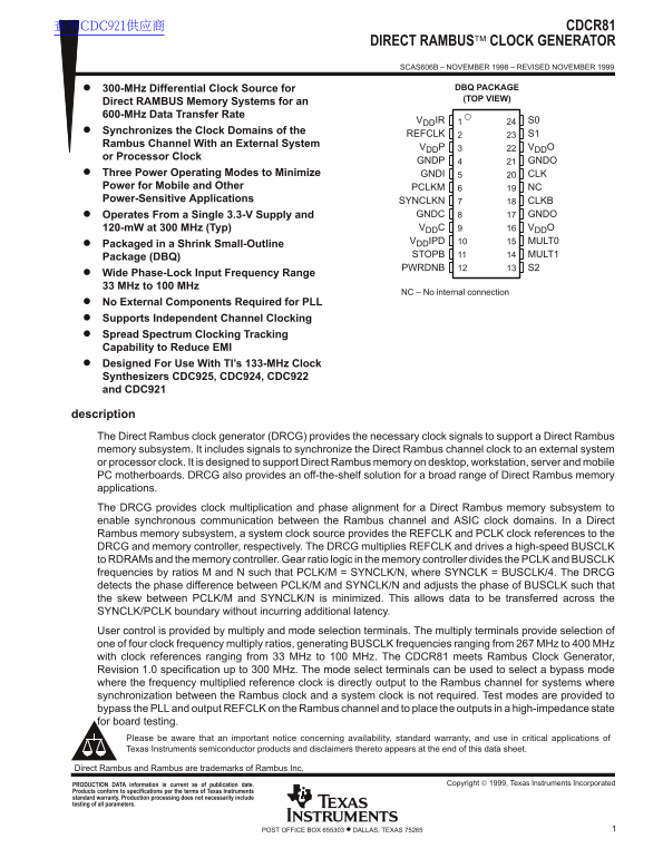
description The Direct Rambus clock generator (DRCG) provides the necessary clock signals to support a Direct Rambus memory subsystem. It includes signals to synchronize the Direct Rambus channel clock to an external system or processor clock. It is designed to support Direct Rambus memory on desktop, workstation, server and mobile PC motherboards. DRCG also provides an off-the-shelf solution for a broad range of Direct Rambus memory applications. The DRCG provides clock multiplication and phase alignment for a Direct Rambus memory subsystem to enable synchronous communication between the Rambus channel and ASIC clock domains. In a Direct Rambus memory subsystem, a system clock source provides the REFCLK and PCLK clock references to the DRCG and memory controller, respectively. The DRCG multiplies REFCLK and drives a high-speed BUSCLK to RDRAMs and the memory controller. Gear ratio logic in the memory controller divides the PCLK and BUSCLK frequencies by ratios M and N such that PCLK/M = SYNCLK/N, where SYNCLK = BUSCLK/4. The DRCG detects the phase difference between PCLK/M and SYNCLK/N and adjusts the phase of BUSCLK such that the skew between PCLK/M and SYNCLK/N is minimized. This allows data to be transferred across the SYNCLK/PCLK boundary without incurring additional latency. User control is provided by multiply and mode selection terminals. The multiply terminals provide selection of one of four clock frequency multiply ratios, generating BUSCLK frequencies ranging from 267 MHz to 400 MHz with clock references ranging from 33 MHz to 100 MHz. The CDCR81 meets Rambus Clock Generator, Revision 1.0 specification up to 300 MHz. The mode select terminals can be used to select a bypass mode where the frequency multiplied reference clock is directly output to the Rambus channel for systems where synchronization between the Rambus clock and a system clock is not required. Test modes are provided to bypass the PLL and output REFCLK on the Rambus channel and to place the outputs in a high-impedance state for board testing.
Please be aware that an important notice concerning availability, standard warranty, and use in critical applications of Texas Instruments semiconductor products and disclaimers thereto appears at the end of this data sheet.
Direct Rambus and Rambus are trademarks of Rambus Inc.
Copyright 1999, Texas Instruments Incorporated PRODUCTION DATA information is current as of publication date.
Products conform to specifications per the terms of Texas Instruments standard warranty. Production processing does not necessarily include testing of all parameters.
1POST OFFICE BOX 655303 • DALLAS, TEXAS 75265
Page Summary Contents For Texas Instruments CDCR81 Direct Rambus Clock Generator Data Sheet
Manual Details
| Brand | Texas Instruments |
|---|---|
| Pages | 13 |
| File Size | 180.69 KB |
| Published | June 02, 2026 |
Enter the captcha to get the download link:

Frequently Asked Questions
How does the CDCR81 synchronize clock domains?
It detects phase differences between PCLK/M and SYNCLK/N, adjusting the phase of BUSCLK to minimize skew for seamless data transfer.
What is the purpose of Bypass mode operation?
Bypass mode outputs the frequency multiplied reference clock directly to the Rambus channel when system synchronization is unnecessary.
What are the operating ranges for the generated clocks?
The reference clocks range from 33 MHz to 100 MHz, and the resulting BUSCLK frequencies vary between 267 MHz and 400 MHz.
How can the device be tested without active PLL operation?
The Function Table details specific combinations of S0, S1, and S2 (like Mode Bypass or Test MUX settings) to bypass the PLL for various board testing requirements.