Texas Instruments CDCF2509 3.3-V Phase-Lock Loop Clock Driver Data Sheet
Summary
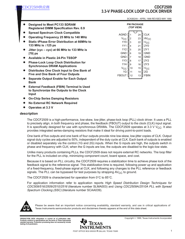
The CDCF2509 is a high-performance, low-skew phase-lock loop (PLL) clock driver designed for synchronous DRAM applications. Operating at 3.3V, this 24-pin TSSOP device distributes one clock input to five and four outputs, offering precise frequency and phase alignment. Ideal for PC133 SDRAM specifications, it features integrated series damping resistors, separate output enables, and a built-in loop filter to minimize component count and board space.
Page 1 Text Content
查询CDCF2509供应商 CDCF2509
3.3-V PHASE-LOCK LOOP CLOCK DRIVER
SCAS624A – APRIL 1999 REVISED MAY 1999
Designed to Meet PC133 SDRAM PW PACKAGE (TOP VIEW)
Registered DIMM Specification Rev. 0.9 Spread Spectrum Clock Compatible
AGND CLK
Operating Frequency 25 MHz to 140 MHz
VCC AVCC
Static t Phase Error Distribution at 66MHz to 1Y0 VCC 133 MHz is ±125 ps 1Y1 2Y0
Jitter (cyc – cyc) at 66 MHz to 133 MHz is 1Y2 2Y1 |70| ps GND GND GND GND
Available in Plastic 24-Pin TSSOP
Phase-Lock Loop Clock Distribution for
Synchronous DRAM Applications
VCC VCC
Distributes One Clock Input to One Bank of
Five and One Bank of Four Outputs
FBOUT FBIN
Separate Output Enable for Each Output Bank External Feedback (FBIN) Terminal Is Used to Synchronize the Outputs to the Clock Input On-Chip Series Damping Resistors No External RC Network Required Operates at 3.3 V
description The CDCF2509 is a high-performance, low-skew, low-jitter, phase-lock loop (PLL) clock driver. It uses a PLL to precisely align, in both frequency and phase, the feedback (FBOUT) output to the clock (CLK) input signal. It is specifically designed for use with synchronous DRAMs. The CDCF2509 operates at 3.3 V VCC. It also provides integrated series-damping resistors that make it ideal for driving point-to-point loads. One bank of five outputs and one bank of four outputs provide nine low-skew, low-jitter copies of CLK. Output signal duty cycles are adjusted to 50%, independent of the duty cycle at CLK. Each bank of outputs is enabled or disabled separately via the control (1G and 2G) inputs. When the G inputs are high, the outputs switch in phase and frequency with CLK; when the G inputs are low, the outputs are disabled to the logic-low state. Unlike many products containing PLLs, the CDCF2509 does not require external RC networks. The loop filter for the PLL is included on-chip, minimizing component count, board space, and cost. Because it is based on PLL circuitry, the CDCF2509 requires a stabilization time to achieve phase lock of the feedback signal to the reference signal. This stabilization time is required, following power up and application of a fixed-frequency, fixed-phase signal at CLK, and following any changes to the PLL reference or feedback signals. The PLL can be bypassed for test purposes by strapping AVCC to ground. The CDCF2509 is characterized for operation from 0°C to 85°C. For application information refer to application reports High Speed Distribution Design Techniques for CDC509/516/2509/2510/2516 (literature number SLMA003) and Using CDC2509A/2510A PLL with Spread Spectrum Clocking (SSC) (literature number SCAA039).
Please be aware that an important notice concerning availability, standard warranty, and use in critical applications of Texas Instruments semiconductor products and disclaimers thereto appears at the end of this data sheet.
PRODUCTION DATA information is current as of publication date. Copyright 1999, Texas Instruments Incorporated
Products conform to specifications per the terms of Texas Instruments standard warranty. Production processing does not necessarily include testing of all parameters.
1POST OFFICE BOX 655303 • DALLAS, TEXAS 75265
Page Summary Contents For Texas Instruments CDCF2509 3.3-V Phase-Lock Loop Clock Driver Data Sheet
Manual Details
| Brand | Texas Instruments |
|---|---|
| Pages | 11 |
| File Size | 138.61 KB |
| Published | June 15, 2026 |
Enter the captcha to get the download link:

Frequently Asked Questions
How do I enable or disable the output banks?
Set 1G or 2G high to enable the corresponding bank; set low to disable outputs to logic-low.
What is the operating frequency range and supply voltage?
Operating frequency is 25 MHz to 140 MHz at 3.3 V VCC.
Does the CDCF2509 require external RC components?
No, the PLL loop filter is on-chip, so no external RC network is needed.
How can I bypass the PLL for testing?
Strap AVCC to ground to bypass the PLL.