Texas Instruments CDC304 OCTAL Divide-by-2 Circuit Clock Driver Data Sheet
Summary
High-performance clock driver and octal divide-by-2 circuit featuring eight low-skew flip-flops, ideal for digital synchronization projects. This comprehensive manual provides electrical characteristics, full operating specifications, package options, and detailed timing parameters necessary for engineers designing robust and reliable clocked circuits. Use this guide to ensure proper integration into high-speed, synchronous electronic systems requiring precise clock stability and control inputs.
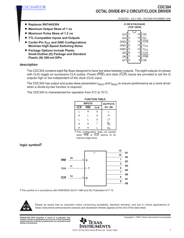
Page 1 Text Content
查询CDC304供应商 CDC304
OCTAL DIVIDE-BY-2 CIRCUIT/CLOCK DRIVER
SCAS325A – JULY 1990 – REVISED NOVEMBER 1995
Replaces SN74AS304 D OR N PACKAGE (TOP VIEW)
Maximum Output Skew of 1 ns Maximum Pulse Skew of 1.5 ns
Q3 Q2 TTL-Compatible Inputs and Outputs Q4 Q1 GND CLR
Center-Pin VCC and GND Configurations
Minimize High-Speed Switching Noise GND VCC GND VCC
Package Options Include Plastic
Q5 CLK
Small-Outline (D) Package and Standard
Q6 PRE
Plastic (N) 300-mil DIPs
description The CDC304 contains eight flip-flops designed to have low skew between outputs. The eight outputs (in-phase with CLK) toggle on successive CLK pulses. Preset (PRE) and clear (CLR) inputs are provided to set the Q outputs high or low independent of the clock (CLK) input. The CDC304 has output and pulse-skew parameters tsk(o) and tsk(p) to ensure performance as a clock driver when a divide-by-two function is required. The CDC304 is characterized for operation from 0°C to 70°C.
FUNCTION TABLE INPUTS OUTPUTS
CLR PRE CLK Q1–Q8
This configuration does not persist when PRE or CLR returns to its inactive (high) level.
logic symbol‡
This symbol is in accordance with ANSI/IEEE Std 91-1984 and IEC Publication 617-12.
Please be aware that an important notice concerning availability, standard warranty, and use in critical applications of Texas Instruments semiconductor products and disclaimers thereto appears at the end of this data sheet.
Copyright 1995, Texas Instruments Incorporated PRODUCTION DATA information is current as of publication date.
Products conform to specifications per the terms of Texas Instruments standard warranty. Production processing does not necessarily include testing of all parameters.
1POST OFFICE BOX 655303 • DALLAS, TEXAS 75265
Page Summary Contents For Texas Instruments CDC304 OCTAL Divide-by-2 Circuit Clock Driver Data Sheet
Manual Details
| Brand | Texas Instruments |
|---|---|
| Pages | 6 |
| File Size | 76.58 KB |
| Published | June 04, 2026 |
Enter the captcha to get the download link:

Frequently Asked Questions
What core function does the CDC304 perform?
It acts as an Octal Divide-by-2 Circuit/Clock Driver, containing eight flip-flops that toggle on successive CLK pulses.
What is the maximum recommended operating clock frequency?
The typical input clock frequency (f) can operate between 0 and a maximum of 80 MHz.
What are the acceptable supply voltage ranges for operation?
The recommended operating supply voltage (Vcc) range is between 4.5 V minimum and 5.5 V maximum.
Can this chip be used in critical life-support systems?
No, the product is not designed or warrantied for use in life-support devices or other critical applications.