Texas Instruments CDC339 Clock Driver with 3-State Outputs
Summary
The CDC339 is a high-performance, low-skew clock distribution and generation driver engineered for complex digital applications. This semi-conductor component provides synchronized outputs at both primary and half frequencies, featuring TTL compatibility and high drive capacity. The accompanying manual serves as a comprehensive resource, detailing electrical specifications, functional diagrams, operating limits, and BiCMOS performance characteristics needed for system design. Ideal for electronic engineers developing reliable clocking circuits where signal integrity and power efficiency are paramount.
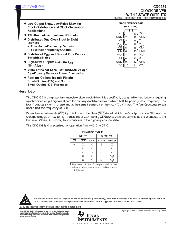
Page 1 Text Content
查询CDC339供应商 CDC339
CLOCK DRIVER WITH 3-STATE OUTPUTS
SCAS331 – DECEMBER 1992 – REVISED MARCH 1994
Low Output Skew, Low Pulse Skew for DB OR DW PACKAGE (TOP VIEW)
Clock-Distribution and Clock-Generation Applications
TTL-Compatible Inputs and Outputs
GND GND
Distributes One Clock Input to Eight
Outputs
VCC VCC
– Four Same-Frequency Outputs
OE CLK
– Four Half-Frequency Outputs
CLR GND
Distributed VCC and Ground Pins Reduce VCC VCC Switching Noise Q4 Q1
High-Drive Outputs (–48-m A IOH, GND GND 48-m A IOL) Q3 Q2
State-of-the-Art EPIC-ΙΙB Bi CMOS Design Significantly Reduces Power Dissipation Package Options Include Plastic Small-Outline (DW) and Shrink Small-Outline (DB) Packages
description The CDC339 is a high-performance, low-skew clock driver. It is specifically designed for applications requiring synchronized output signals at both the primary clock frequency and one-half the primary clock frequency. The four Y outputs switch in phase and at the same frequency as the clock (CLK) input. The four Q outputs switch at one-half the frequency of CLK. When the output-enable (OE) input is low and the clear (CLR) input is high, the Y outputs follow CLK and the Q outputs toggle on low-to-high transitions of CLK. Taking CLR low asynchronously resets the Q outputs to the low level. When OE is high, the outputs are in the high-impedance state. The CDC339 is characterized for operation from –40°C to 85°C.
FUNCTION TABLE INPUTS OUTPUTS
OE CLR CLK Y1–Y4 Q1–Q4
The level of the Q outputs before the indicated steady-state input conditions were established.
Please be aware that an important notice concerning availability, standard warranty, and use in critical applications of Texas Instruments semiconductor products and disclaimers thereto appears at the end of this data sheet.
EPIC-ΙΙB is a trademark of Texas Instruments Incorporated.
Copyright 1994, Texas Instruments Incorporated PRODUCTION DATA information is current as of publication date.
Products conform to specifications per the terms of Texas Instruments standard warranty. Production processing does not necessarily include testing of all parameters.
1POST OFFICE BOX 655303 • DALLAS, TEXAS 75265
Page Summary Contents For Texas Instruments CDC339 Clock Driver with 3-State Outputs
Manual Details
| Brand | Texas Instruments |
|---|---|
| Pages | 7 |
| File Size | 92.39 KB |
| Published | June 01, 2026 |
Enter the captcha to get the download link:

Frequently Asked Questions
What is the operating principle of the CDC339 clock outputs?
The four Y outputs switch at the primary frequency of CLK, while the four Q outputs switch at one-half the primary clock frequency.
In what state do I configure OE and CLR for normal operation?
For the Y outputs to follow CLK, the Output-Enable (OE) input must be low and the Clear (CLR) input must be high.
What is the recommended temperature range for this clock driver?
The device is characterized for stable operation from –40°C to 85°C.
Are these semiconductors suitable for critical life-support systems?
No, TI products are not designed or warranted for use in life-support devices or other critical applications.