Fairchild MM74HC4046 CMOS Phase Lock Loop Data Handbook
Summary
The MM74HC4046 is a low power CMOS Phase Lock Loop (PLL) featuring a voltage-controlled oscillator (VCO), three phase comparators, and a source follower. Designed for high frequency operation up to 12 MHz, this 16-pin integrated circuit provides high linearity and fast response, ideal for frequency synthesis, demodulation, and clock recovery applications.
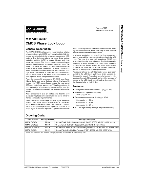
Page 1 Text Content
74H 4046 C ase L ck L
February 1984 Revised October 2003
MM74HC4046 CMOS Phase Lock Loop
them. This comparator is more susceptible to noise throw-
General Description
ing the loop out of lock, but is less likely to lock onto har-
The MM74HC4046 is a low power phase lock loop utilizing
monics than the other two comparators.
advanced silicon-gate CMOS technology to obtain high fre-
In a typical application any one of the three comparators
quency operation both in the phase comparator and VCO
feed an external filter network which in turn feeds the VCO
sections. This device contains a low power linear voltage
input. This input is a very high impedance CMOS input
controlled oscillator (VCO), a source follower, and three
which also drives the source follower. The VCO’s operating
phase comparators. The three phase comparators have a
frequency is set by three external components connected
common signal input and a common comparator input. The
to the C1A, C1B, R1 and R2 pins. An inhibit pin is provided
signal input has a self biasing amplifier allowing signals to
to disable the VCO and the source follower, providing a
be either capacitively coupled to the phase comparators
method of putting the IC in a low power state.
with a small signal or directly coupled with standard input
The source follower is a MOS transistor whose gate is con-
logic levels. This device is similar to the CD4046 except
nected to the VCO input and whose drain connects the
that the Zener diode of the metal gate CMOS device has
been replaced with a third phase comparator. Demodulator output. This output normally is used by tying a resistor from pin 10 to ground, and provides a means of
Phase Comparator I is an exclusive OR (XOR) gate. It pro-
looking at the VCO input without loading down modifying
vides a digital error signal that maintains a 90 phase shift
the characteristics of the PLL filter.
between the VCO’s center frequency and the input signal (50% duty cycle input waveforms). This phase detector is
more susceptible to locking onto harmonics of the input fre- Features
quency than phase comparator I, but provides better noise ■Low dynamic power consumption: (VCC = 4.5V) rejection.
■Maximum VCO operating frequency:
Phase comparator III is an SR flip-flop gate. It can be used
12 MHz (VCC = 4.5V)
to provide the phase comparator functions and is similar to
■Fast comparator response time (VCC = 4.5V)
the first comparator in performance.
Phase comparator II is an edge sensitive digital sequential Comparator I: 25 ns
network. Two signal outputs are provided, a comparator Comparator II: 30 ns output and a phase pulse output. The comparator output is
Comparator III: 25 ns
a 3-STATE output that provides a signal that locks the VCO
■VCO has high linearity and high temperature stability
output signal to the input signal with 0 phase shift between
Ordering Code: Order Number Package Number Package Description MM74HC4046M M16A 16-Lead Small Outline Integrated Circuit (SOIC), JEDEC MS-012, 0.150" Narrow MM74HC4046SJ M16D 16-Lead Small Outline Package (SOP), EIAJ TYPE II, 5.3mm Wide MM74HC4046MTC MTC16 16-Lead Thin Shrink Small Outline Package (TSSOP), JEDEC MO-153, 4.4mm Wide MM74HC4046N N16E 16-Lead Plastic Dual-In-Line Package (PDIP), JEDEC MS-001, 0.300" Wide Devices also available in Tape and Reel. Specify by appending the suffix letter “X” to the ordering code.
© 2003 Fairchild Semiconductor Corporation DS005352 www.fairchildsemi.com
Page Summary Contents For Fairchild MM74HC4046 CMOS Phase Lock Loop Data Handbook
Manual Details
| Brand | Fairchild |
|---|---|
| Pages | 17 |
| File Size | 250.92 KB |
| Published | June 15, 2026 |
Enter the captcha to get the download link:

Frequently Asked Questions
How many phase comparators does the MM74HC4046 have and what are their types?
It has three phase comparators: Phase Comparator I (XOR gate), Phase Comparator II (edge-sensitive sequential network with 3-STATE output), and Phase Comparator III (SR flip-flop).
What is the maximum VCO operating frequency of the MM74HC4046?
The maximum VCO operating frequency is 12 MHz at VCC = 4.5V.
How can I put the MM74HC4046 into a low power state?
Use the inhibit pin to disable the VCO and source follower, putting the IC in a low power state.
What are the recommended supply voltage and operating temperature ranges?
Supply voltage (VCC) 2V to 6V, operating temperature -40°C to +85°C.