Motorola Semiconductor MMBTH10LT1 Data Handbook/Sheet
Summary
Discover comprehensive technical data for the MMBTH10LT1/D, an NPN Silicon Bipolar Junction Transistor (BJT). This datasheet provides expert specifications on crucial operational parameters, including electrical characteristics, thermal dissipation limits, breakdown voltages, and high-frequency performance metrics. It is essential reading for electronics engineers and circuit designers who require reliable component selection and detailed validation data when integrating small-signal solid-state components into their designs.
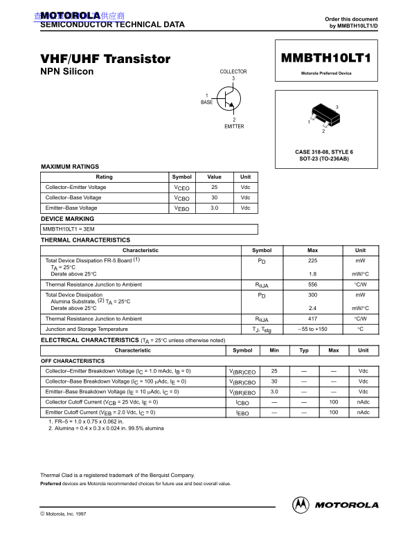
Page 1 Text Content
查询MMBTH10LT1供应商
Order this document
SEMICONDUCTOR TECHNICAL DATA by MMBTH10LT1/D
NPN Silicon COLLECTOR Motorola Preferred Device
EMITTER
CASE 318-08, STYLE 6 SOT-23 (TO-236AB)
MAXIMUM RATINGS
Rating Symbol Value Unit
Collector–Emitter Voltage VCEO Vdc Collector–Base Voltage VCBO Vdc Emitter–Base Voltage VEBO 3.0 Vdc
DEVICE MARKING MMBTH10LT1 = 3EM THERMAL CHARACTERISTICS
Characteristic Symbol Max Unit
Total Device Dissipation FR-5 Board (1) PD m W TA = 25°C Derate above 25°C 1.8 m W/°C Thermal Resistance Junction to Ambient RθJA °C/W Total Device Dissipation PD m W Alumina Substrate, (2) TA = 25°C Derate above 25°C 2.4 m W/°C Thermal Resistance Junction to Ambient RθJA °C/W Junction and Storage Temperature TJ, Tstg –55 to +150 °C
ELECTRICAL CHARACTERISTICS (TA = 25°C unless otherwise noted)
Characteristic Symbol Min Typ Max Unit
OFF CHARACTERISTICS Collector–Emitter Breakdown Voltage (IC = 1.0 m Adc, IB = 0) V(BR)CEO Vdc Collector–Base Breakdown Voltage (IC = 100 µAdc, IE = 0) V(BR)CBO Vdc Emitter–Base Breakdown Voltage (IE = 10 µAdc, IC = 0) V(BR)EBO 3.0 Vdc Collector Cutoff Current (VCB = 25 Vdc, IE = 0) ICBO n Adc Emitter Cutoff Current (VEB = 2.0 Vdc, IC = 0) IEBO n Adc 1. FR–5 = 1.0 x 0.75 x 0.062 in. 2. Alumina = 0.4 x 0.3 x 0.024 in. 99.5% alumina
Thermal Clad is a registered trademark of the Berquist Company. Preferred devices are Motorola recommended choices for future use and best overall value.
1Motorola Small–Signal Transistors, FETs and Diodes Device Data
Motorola, Inc. 1997
Page Summary Contents For Motorola Semiconductor MMBTH10LT1 Data Handbook/Sheet
Manual Details
| Brand | Motorola |
|---|---|
| Pages | 6 |
| File Size | 89.70 KB |
| Published | May 29, 2026 |
Enter the captcha to get the download link:

Frequently Asked Questions
What is the maximum acceptable Collector–Emitter Voltage (Vce)?
The maximum collector-emitter voltage rating (CEO) is 25 Vdc.
Which physical package type (Style) should be used for surface mounting?
The device comes in Style 6, which uses a SOT-23 package.
How is the power dissipation of this SOT–23 package affected in application?
Power dissipation depends on the soldering pad size and drain pad size, not just the minimum pads.
What is the typical DC current gain (hFE) when operating at 4.0 mAdc and 10 Vdc?
The typical DC current gain (hFE) listed for these conditions is 60.