MOTOROLA 33702 Data Sheet / Handbook
Summary
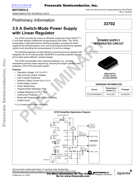
This comprehensive technical manual details the MC33702, a high-efficiency switch-mode power supply designed for stable voltage regulation in advanced embedded systems. The device efficiently supplies core and I/O voltages for Motorola microprocessors and DSPs using combined buck and low dropout (LDO) technology. This resource provides engineers with critical specifications, including detailed pin descriptions, multi-stage power sequencing features, overcurrent protection, and operating parameters (2.8 V to 6.0 V). It is the essential guide for designers building complex digital circuits requiring precise and reliable power delivery.
Page 1 Text Content
re sc le ic to r,
查询33702供应商 Freescale Semiconductor, Inc.
MOTOROLA Order this document from Analog Marketing: MC33702/D
Rev 0, 05/2003
SEMICONDUCTOR TECHNICAL DATA
Preliminary Information
3.0 A Switch-Mode Power Supply with Linear Regulator The 33702 provides the means to efficiently supply the Power QUICC™ I,
II, and other families of Motorola microprocessors and DSPs. The 33702 POWER SUPPLY
incorporates a high-performance switching regulator, providing the direct INTEGRATED CIRCUIT supply for the microprocessor’s core, and a low dropout (LDO) linear regulator control circuit providing the microprocessor I/O and bus voltage. The switching regulator is a high-efficiency synchronous buck regulator with integrated 50 mΩ N-channel power MOSFETs to provide protection features and to allow space-efficient, compact design. The 33702 incorporates many advanced features; e.g., precisely maintained up/down power sequencing, ensuring the proper operation and protection of the CPU and power system. Features Operating Voltage: 2.8 V to 6.0
DWB SUFFIX
High-Accuracy Output Voltages
CASE 1324-02
Fast Transient Response 32-LEAD SOICW Switcher Output Current Up to 3.0 Undervoltage Lockout
ORDERING INFORMATION
Power Sequencing Programmable Watchdog Timer
Device Temperature Package
Range (TA)
Voltage Margining via I2C™ Bus
Overcurrent Protection PC33702DWB/R2 -40 to 85°C 32 SOICW
Reset with Programmable Power-ON Delay Enable Inputs
I2C is a trademark of Phillips Corporation.
33702 Simplified Application Diagram 2.8 .8 V to 6.0 to 13.5 In put
VIN2 VIN1 IN1
Othe Circuits
VBD BD VBST BST
VLDO =
SR 0.8 to 5.0 RT (Adjustable)
LDO VDDH (I/Os)
ADDR LFB
MPC85xx XXX
SDA SCL
RESET PORESET
GND VOUT =
BOOT VBST
0.8 to 5.0 EN1 (Adjustable)
EN2 VDDL (Core)SW
VOUT VO
CLKSYN
CLKSEL PGND
Optional
This document contains information on a product under development. Motorola reserves the right to change or discontinue this product without notice.
For More Information On This Product,
© Motorola, Inc. 2003
Go to: www.freescale.com
Page Summary Contents For MOTOROLA 33702 Data Sheet / Handbook
Manual Details
| Brand | Motorola |
|---|---|
| Pages | 24 |
| File Size | 641.19 KB |
| Published | June 01, 2026 |
Enter the captcha to get the download link:

Frequently Asked Questions
What types of power conversion does the 33702 provide?
It includes a high-efficiency synchronous buck regulator for the core supply and an LDO linear regulator for I/O and bus voltage.
Does the chip handle multiple power stages?
Yes, it provides precisely maintained up/down power sequencing to ensure proper operation of the CPU and power system features.
What is the operating frequency default setting?
The default switching frequency (when the FREQ pin is left open or tied to VDD) is set to 300 kHz.
Can this product be used in life support systems?
No, it is not designed for use in surgical implants or other applications where failure could cause personal injury or death.