MOTOROLA MRFIC0913 Data Handbook
Summary
This integrated circuit is a high-performance Power Amplifier designed specifically for use in GSM Class IV cellular handsets operating within the 800 to 1000 MHz band. Utilizing advanced GaAs MESFET technology, it ensures superior signal amplification and thermal efficiency critical for mobile communications. This document provides comprehensive technical specifications, including absolute maximum ratings, recommended operating ranges, detailed electrical characteristics (Output Power, PAE), and functional application circuits necessary for integrating the device into complex mobile communication systems.
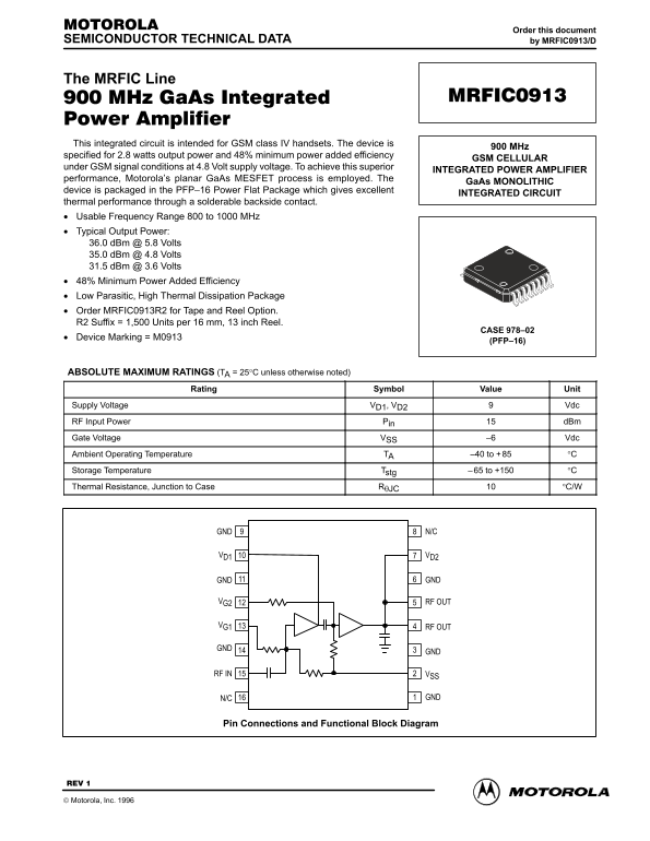
Page 1 Text Content
Order this document
SEMICONDUCTOR TECHNICAL DATA by MRFIC0913/D
This integrated circuit is intended for GSM class IV handsets. The device is
900 MHz
specified for 2.8 watts output power and 48% minimum power added efficiency
GSM CELLULAR
under GSM signal conditions at 4.8 Volt supply voltage. To achieve this superior
INTEGRATED POWER AMPLIFIER
performance, Motorola’s planar Ga As MESFET process is employed. The
Ga As MONOLITHIC
device is packaged in the PFP–16 Power Flat Package which gives excellent
INTEGRATED CIRCUIT
thermal performance through a solderable backside contact. Usable Frequency Range 800 to 1000 MHz Typical Output Power: 36.0 d Bm @ 5.8 Volts 35.0 d Bm @ 4.8 Volts 31.5 d Bm @ 3.6 Volts 48% Minimum Power Added Efficiency Low Parasitic, High Thermal Dissipation Package Order MRFIC0913R2 for Tape and Reel Option. R2 Suffix = 1,500 Units per 16 mm, 13 inch Reel.
CASE 978–02
Device Marking = M0913
(PFP–16)
ABSOLUTE MAXIMUM RATINGS (TA = 25°C unless otherwise noted)
Rating Symbol Value Unit
Supply Voltage VD1, VD2 Vdc RF Input Power Pin d Bm Gate Voltage VSS –6 Vdc Ambient Operating Temperature TA –40 to +85 °C Storage Temperature Tstg –65 to +150 °C Thermal Resistance, Junction to Case RθJC °C/W
GND N/C
VD1 VD2
GND GND
VG2 RF OUT
VG1 RF OUT
RF IN VSS
N/C GND
Pin Connections and Functional Block Diagram
Motorola, Inc. 1996
MRFIC0913MOTOROLA RF DEVICE DATA
Page Summary Contents For MOTOROLA MRFIC0913 Data Handbook
Manual Details
| Brand | Motorola |
|---|---|
| Pages | 8 |
| File Size | 140.57 KB |
| Published | June 04, 2026 |
Enter the captcha to get the download link:

Frequently Asked Questions
What is the standard operating temperature range?
The ambient operating temperature (T) is –40 to +85°C. The storage temperature (T stg) is –65 to +150°C.
Which package is used, and what are its benefits?
It is packaged in the PFP–16 Power Flat Package, which provides excellent thermal performance through a solderable backside contact.
What input frequency range should be used?
The usable frequency range is 800 to 1000 MHz, and the recommended operating range is 880 to 915 MHz.
Does the unit have specific voltage requirements for operation?
It operates with a supply voltage (V D1 D2) between 2.7 to 7.5 Vdc when powered through the main connection pins.