Motorola Semiconductor MC10E150 MC100E150 Data Sheet User Manual
Summary
The MC10E/100E150 is a high-performance 6-bit D Latch featuring differential outputs, designed for reliable data capture in advanced digital circuits. This technical manual provides engineers and electronics designers with exhaustive operational specifications, including full pinouts, detailed DC/AC electrical characteristics (timing diagrams, propagation delays), and package information. Use this resource to guarantee precise integration of stable, low-power latching capabilities into your next hardware design.
Page 1 Text Content
SEMICONDUCTOR TECHNICAL DATA
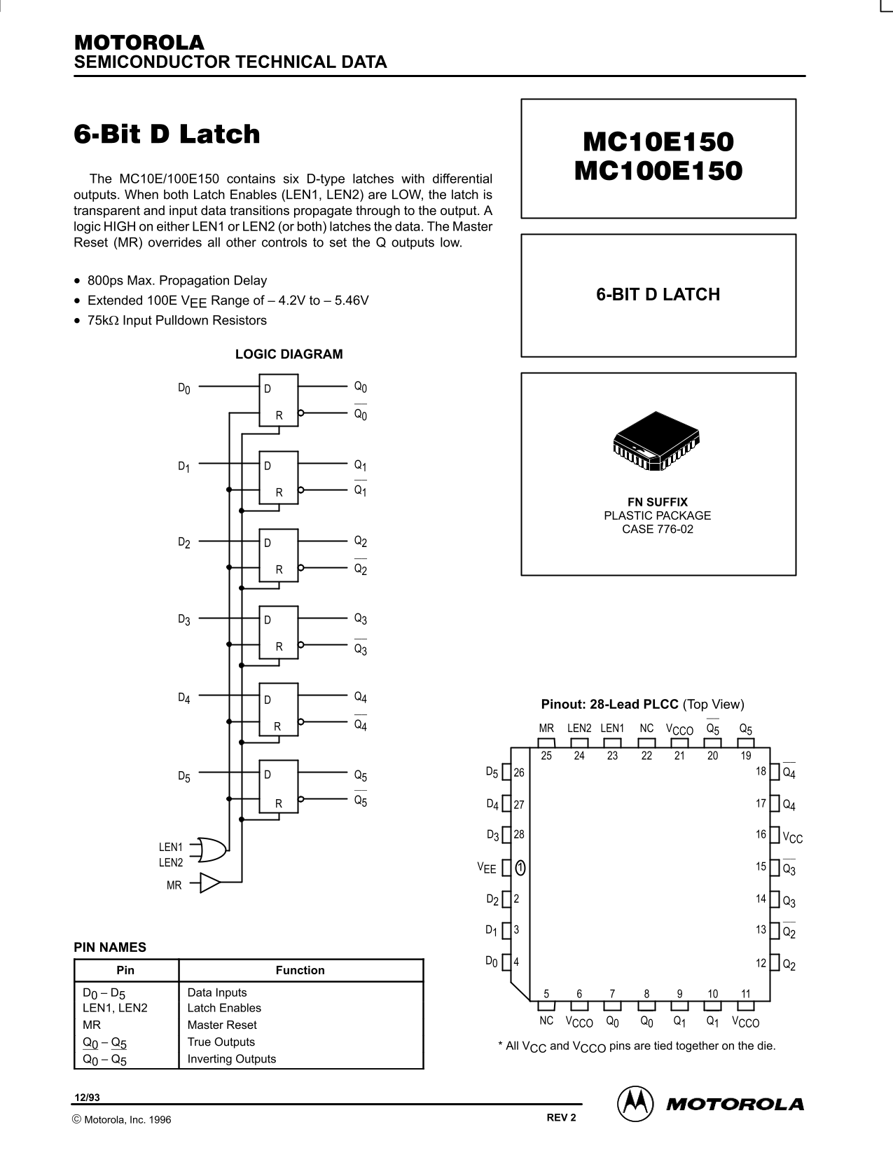
The MC10E/100E150 contains six D-type latches with differential outputs. When both Latch Enables (LEN1, LEN2) are LOW, the latch is transparent and input data transitions propagate through to the output. A logic HIGH on either LEN1 or LEN2 (or both) latches the data. The Master Reset (MR) overrides all other controls to set the Q outputs low.
800ps Max. Propagation Delay
6-BIT D LATCH
Extended 100E VEE Range of – 4.2V to – 5.46V 75kΩ Input Pulldown Resistors
LOGIC DIAGRAM
FN SUFFIX PLASTIC PACKAGE CASE 776-02
Pinout: 28-Lead PLCC (Top View)
Q5Q5VCCONCLEN1LEN2MR
D3 VCC
LEN1 LEN2
VEE Q3
PIN NAMES
Pin Function D0 D5 Data Inputs LEN1, LEN2 Latch Enables
NC VCCO Q0 Q0 Q1 Q1 VCCO
MR Master Reset Q0 Q5 True Outputs
* All VCC and VCCO pins are tied together on the die.
Q0 Q5 Inverting Outputs
2–1 REV 2 Motorola, Inc. 1996
Page Summary Contents For Motorola Semiconductor MC10E150 MC100E150 Data Sheet User Manual
Manual Details
| Brand | Motorola |
|---|---|
| Pages | 5 |
| File Size | 65.33 KB |
| Published | July 15, 2026 |
Enter the captcha to get the download link:

Frequently Asked Questions
What happens when I set both Latch Enables (LEN1, LEN2) to LOW?
The latch is transparent, allowing input data transitions to propagate directly to the output.
How can I ensure the outputs are set low regardless of other controls?
Applying a logic HIGH on Master Reset (MR) overrides all other controls and sets the Q outputs low.
What material package does this component use?
It comes in a PLCC plastic package case 776-02 and has a 28-Lead layout.
What is the required logic high input current for LEN or MR pins?
The typical minimum required input current (IH) is 150 μA across all stated conditions.