Motorola Semiconductor MC10E142 MC100E142 Data Sheet
Summary
This technical summary details the MC10E/MC100E 9-bit shift register, a foundational memory component designed for robust byte-parity applications in digital electronics. The manual provides comprehensive coverage of its dual-clock functionality, mode selection (load vs. shift), electrical specifications, timing parameters, and operational guidelines for minimizing noise and maximizing reliability. This integrated circuit is essential for hardware engineers, embedded systems designers, and professionals requiring reliable synchronous logic control elements for advanced circuit prototyping and manufacturing.
Page 1 Text Content
查询MC100E142供应商 SEMICONDUCTOR TECHNICAL DATA
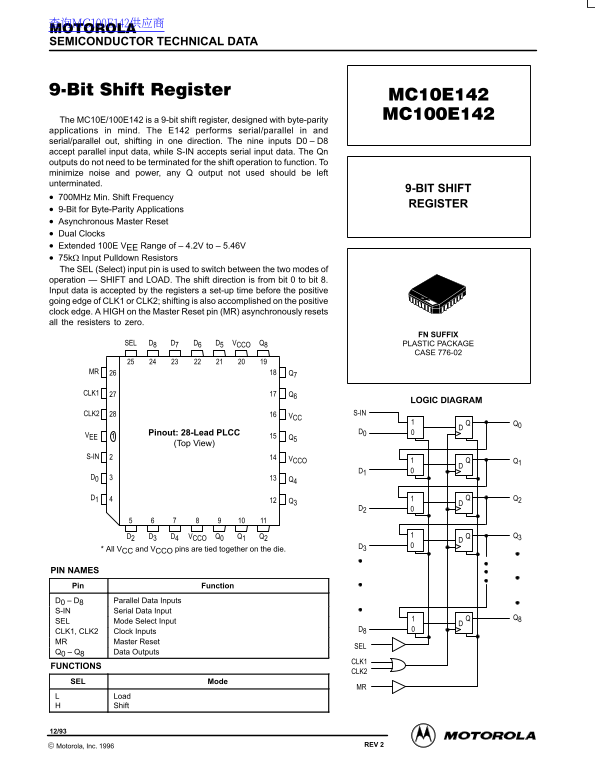
The MC10E/100E142 is a 9-bit shift register, designed with byte-parity applications in mind. The E142 performs serial/parallel in and serial/parallel out, shifting in one direction. The nine inputs D0 D8 accept parallel input data, while S-IN accepts serial input data. The Qn outputs do not need to be terminated for the shift operation to function. To minimize noise and power, any Q output not used should be left unterminated.
9-BIT SHIFT
700MHz Min. Shift Frequency
REGISTER
9-Bit for Byte-Parity Applications Asynchronous Master Reset Dual Clocks Extended 100E VEE Range of – 4.2V to – 5.46V 75kΩ Input Pulldown Resistors The SEL (Select) input pin is used to switch between the two modes of operation — SHIFT and LOAD. The shift direction is from bit 0 to bit 8. Input data is accepted by the registers a set-up time before the positive going edge of CLK1 or CLK2; shifting is also accomplished on the positive clock edge. A HIGH on the Master Reset pin (MR) asynchronously resets all the resisters to zero.
FN SUFFIX
VCCOD5D6D7D8SEL Q8 PLASTIC PACKAGE
CASE 776-02
MR Q7
CLK1 Q6
LOGIC DIAGRAM
CLK2 S-IN
Pinout: 28-Lead PLCC D0
(Top View)
D2 D3 D4 VCCO Q0 Q1 Q2 Q3
* All VCC and VCCO pins are tied together on the die.
PIN NAMES Pin Function D0 – D8 Parallel Data Inputs S-IN Serial Data Input
SEL Mode Select Input
CLK1, CLK2 Clock Inputs MR Master Reset
Q0 – Q8 Data Outputs
FUNCTIONS
SEL Mode
Load Shift
2–1 REV 2 Motorola, Inc. 1996
Page Summary Contents For Motorola Semiconductor MC10E142 MC100E142 Data Sheet
Manual Details
| Brand | Motorola |
|---|---|
| Pages | 4 |
| File Size | 110.29 KB |
| Published | June 04, 2026 |
Enter the captcha to get the download link:

Frequently Asked Questions
How does the MC10E/MC100E work for data transfer?
It is a 9-bit shift register designed to accept parallel input via D0-D8 or serial input via S-IN.
What are the operational modes and how do I switch between them?
The SEL pin controls the mode between SHIFT and LOAD. CLK1/CLK2 clocks handle both shifts and loading operations.
How can I asynchronously reset the unit?
Apply a HIGH signal to the Master Reset (MR) pin to synchronously reset all registers to zero.
What is the maximum operating frequency for shifting?
The maximum shift frequency (f Max. Shift Frequency) is 700 MHz, with an optimal range of 900 MHz.