Motorola MC74AC109 MC74ACT109 Data Manual
Summary
This technical guide provides comprehensive specifications for the MC74AC109/74ACT109, a dual JK high-speed flip-flop essential for advanced digital circuit design. The documentation details functional operation, including logic diagrams, truth tables, and crystal-clear operating parameters across varying temperatures and voltages. It covers maximum ratings, recommended electrical characteristics (DC/AC), ensuring engineers have all necessary data to reliably integrate this stable, independent JK logic element into their hardware systems.
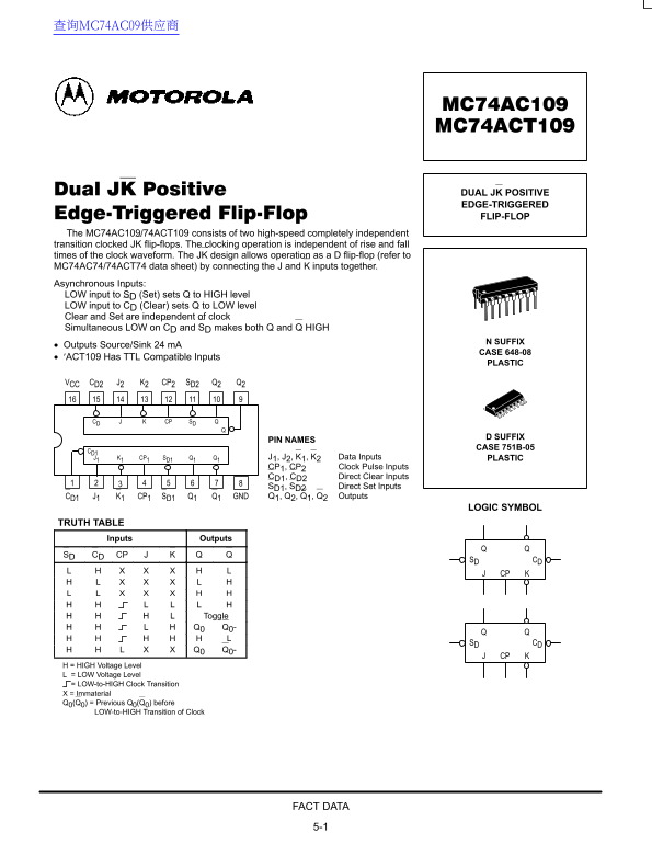
Page 1 Text Content
查询MC74AC09供应商
DUAL JK POSITIVE EDGE-TRIGGERED FLIP-FLOP
The MC74AC109/74ACT109 consists of two high-speed completely independent transition clocked JK flip-flops. The clocking operation is independent of rise and fall times of the clock waveform. The JK design allows operation as a D flip-flop (refer to MC74AC74/74ACT74 data sheet) by connecting the J and K inputs together. Asynchronous Inputs: LOW input to SD (Set) sets Q to HIGH level LOW input to CD (Clear) sets Q to LOW level Clear and Set are independent of clock Simultaneous LOW on CD and SD makes both Q and Q HIGH
N SUFFIX
Outputs Source/Sink 24 m A
CASE 648-08
′ACT109 Has TTL Compatible Inputs
PLASTIC
VCC CD2 J2 K2 CP2 SD2 Q2 Q2
CD CP SD
D SUFFIX
PIN NAMES
CASE 751B-05
J1 K1 CP1 SD1 Q1 Q1 J1, J2, K1, K2 Data Inputs PLASTIC CP1, CP2 Clock Pulse Inputs CD1, CD2 Direct Clear Inputs SD1, SD2 Direct Set Inputs CD1 J1 K1 CP1 SD1 Q1 Q1 GND Q1, Q2, Q1, Q2 Outputs
LOGIC SYMBOL
TRUTH TABLE
Inputs Outputs
SD CD CP
SD CD
Toggle Q0 Q0-
SD CD
H = HIGH Voltage Level L = LOW Voltage Level = LOW-to-HIGH Clock Transition X = Immaterial Q0(Q0) = Previous Q0(Q0) before
LOW-to-HIGH Transition of Clock
FACT DATA 5-1
Page Summary Contents For Motorola MC74AC109 MC74ACT109 Data Manual
Manual Details
| Brand | Motorola |
|---|---|
| Pages | 6 |
| File Size | 199.54 KB |
| Published | June 01, 2026 |
Enter the captcha to get the download link:
