# A B C D E F G H I J K L M N O P Q R S T U V W X Y Z

Motorola XC33989 Data Sheet/Manual

Summary

The MC33989 is a critical system basis chip and high-speed CAN transceiver designed specifically for advanced automotive Electronic Control Units (ECUs). This specialized integrated circuit manages complex functions, including reliable 1Mbaud CAN communication, dual voltage regulation, and multiple external wake-up inputs. The manual provides detailed technical ratings, electrical characteristics, operating parameters across various power modes, and pin connection specifications. It is the essential resource for automotive embedded system engineers developing reliable vehicle control systems requiring robust connectivity and precise power management.
📄 Preview PAGE OF 32

Page 1 Text Content

re sc le ic to r,

查询PC33989DW供应商 Order this document by Rev: 4.91 Date: 10th July, 2002

MOTOROLA

Freescale Semiconductor, Inc.

SEMICONDUCTOR

XC33989

TECHNICAL DATA Advance Information

System Basis Chip with SYSTEM BASIS CHIP WITH HIGH SPEED CAN

High Speed CAN Transceiver

SEMICONDUCTOR TECHNICAL DATA

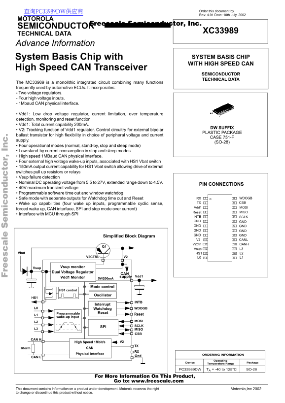
The MC33989 is a monolithic integrated circuit combining many functions frequently used by automotive ECUs. It incorporates: - Two voltage regulators. - Four high voltage inputs. - 1Mbaud CAN physical interface.

Vdd1: Low drop voltage regulator, current limitation, over temperature detection, monitoring and reset function Vdd1: Total current capability 200m A.

DW SUFFIX

V2: Tracking function of Vdd1 regulator. Control circuitry for external bipolar

PLASTIC PACKAGE

ballast transistor for high flexibility in choice of peripheral voltage and current

CASE 751-F

supply.

(SO-28)

Four operational modes (normal, stand-by, stop and sleep mode) Low stand-by current consumption in stop and sleep modes High speed 1MBaud CAN physical interface. Four external high voltage wake-up inputs, associated with HS1 Vbat switch 150m A output current capability for HS1 Vbat switch allowing drive of external switches pull up resistors or relays Vsup failure detection Nominal DC operating voltage from 5.5 to 27V, extended range down to 4.5V.

PIN CONNECTIONS

40V maximum transient voltage Programmable software time out and window watchdog

Safe mode with separate outputs for Watchdog time out and Reset RX WDOGB

TX CSB

Wake up capabilities (four wake up inputs, programmable cyclic sense,

Vdd1 MOSI

forced wake up, CAN interface, SPI and stop mode over current)

Reset MISO

Interface with MCU through SPI

INTB SCLK

GNDGND

GND GND GND GND GND GND

Simplified Block Diagram

V2 CANL V2ctrl CANH

Vsup L3

Vbat HS1 L2

V2CTRL V2 L0 L1

Vsup monitor

Dual Voltage Regulator

supply Vdd1

Vdd1 Monitor

Mode control

HS1 control

Oscillator

Interrupt

L0 Watchdog WDOGB

Programmable Reset

L1 Reset

wake-up input

L2 MOSI SCLK

L3 MISO

CAN H

V2 High Speed 1Mbit/s

Rterm CAN

Physical Interface ORDERING INFORMATION

CAN L

Operating

Device Package

Temperature Range

SO-28TA = -40 to 125°CPC33989DW

For More Information On This Product, Go to: www.freescale.com

This document contains information on a product under development. Motorola reserves the right Motorola,Inc 2002 to change or discontinue this product without notice.

Page Summary Contents For Motorola XC33989 Data Sheet/Manual

Page 1 re sc le ic to r, 查询PC33989DW供应商 Order this document by Rev: 4.91 Date: 10th July, 2002 MOTOROLA Freescale Semiconductor, Inc. SEMICONDUCTOR XC33989 TECHNICAL DATA Advance Information System Basis Chi...
Page 2 re sc le ic to r, MC33989 Freescale Semiconductor, Inc. MAXIMUM RATINGS Ratings Symbol Min Typ Max Unit ELECTRICAL RATINGS Supply Voltage at Vsup - Continuous voltage Vsup -0.3 - Transient voltage (Lo...
Page 3 re sc le ic to r, MC33989 Freescale Semiconductor, Inc. ELECTRICAL CHARACTERISTICS (Vsup From 5.5V to 18V and Tamb -40°C to 125°C) For all pins except CANH, CANL, Tx and Rx which are described in the ...
Page 4 re sc le ic to r, MC33989 Freescale Semiconductor, Inc. (Vsup From 5.5V to 18V and Tamb -40°C to 125°C) For all pins except CANH, CANL, Tx and Rx which are described in the CAN module section Characte...
Page 5 re sc le ic to r, MC33989 Freescale Semiconductor, Inc. (Vsup From 5.5V to 18V and Tamb -40°C to 125°C) For all pins except CANH, CANL, Tx and Rx which are described in the CAN module section Characte...
Page 6 re sc le ic to r, MC33989 Freescale Semiconductor, Inc. (Vsup From 5.5V to 18V and Tamb -40°C to 125°C) For all pins except CANH, CANL, Tx and Rx which are described in the CAN module section Characte...
Page 7 re sc le ic to r, MC33989 Freescale Semiconductor, Inc. (Vsup From 5.5V to 18V and Tamb -40°C to 125°C) For all pins except CANH, CANL, Tx and Rx which are described in the CAN module section Characte...
Page 8 re sc le ic to r, MC33989 Freescale Semiconductor, Inc. CAN MODULE SPECIFICATION MAXIMUM RATING Ratings Symbol Min Typ Max Unit ELECTRICAL RATINGS CANL,CANH Continuous voltage Vcan H,L -27 CANL,CANH C...
Page 9 re sc le ic to r, MC33989 Freescale Semiconductor, Inc. DEVICE DESCRIPTION Descriptions Symbol Min Typ Max Unit Conditions CAN H output current capability Icanh -35 m A Dominant state CAN L output cur...
Page 10 re sc le ic to r, MC33989 Freescale Semiconductor, Inc. DEVICE DESCRIPTION Figure 3. Transient test pulses for CANH and CANL CAN H Transient Pulse Generator (note) CAN L 1n F Gnd note: Waveform in acc...
Page 11 re sc le ic to r, MC33989 Freescale Semiconductor, Inc. diagram to be inserted Figure 5. Wake up block diagram The block diagram illustrates how the wake up signal is generated. First the CAN signal i...
Page 12 re sc le ic to r, MC33989 Freescale Semiconductor, Inc. GENERAL DESCRIPTION The MC33989 is an integrated circuit dedicated to automotive applications. It includes the following functions: - One full p...
Page 13 re sc le ic to r, MC33989 Freescale Semiconductor, Inc. 4.7.2.2 Normal request entered and no W/D configuration occurs: In case the Normal request mode is entered after SBC power up or after a wake up...
Page 14 re sc le ic to r, MC33989 Freescale Semiconductor, Inc. Once stop mode is entered the SBC could wake up from the V1 regulator over current detection. In order to allow time for the MCU to complete the...
Page 15 re sc le ic to r, MC33989 Freescale Semiconductor, Inc. WDOGB Reset Events Mode output output Vdd1 < Rst-th high low Watchdog time out reached low (note1) low - Vdd1 normal 2 (safe mode) high high ...
Page 16 re sc le ic to r, MC33989 Freescale Semiconductor, Inc. and Tx pins are compatible to ISO11898 specification (IS0 11898: 1993(E)). The control of the CAN physical interface operation is done through t...
Page 17 re sc le ic to r, MC33989 Freescale Semiconductor, Inc. Figure 7. Simplified schematic for Flash programming Simplified connection used in Flash programming mode Vsup (open or >5V reset Programming...
Page 18 re sc le ic to r, MC33989 Freescale Semiconductor, Inc. TABLE OF OPERATION The table below describes the SBC operation modes. “Normal Debug”, “Standby Debug” and “Stop Debug” are entered via special s...
Page 19 re sc le ic to r, MC33989 Freescale Semiconductor, Inc. STATE MACHINE State machine (not valid in debug modes) SB ow er W/D: timeout OR Vdd1 low W/D: timeout & Nostop & !BATFAIL Reset counter ...
Page 20 re sc le ic to r, MC33989 Freescale Semiconductor, Inc. Transitions to enter debug modes SP I: St op W/D: time out 350ms Power Normal Request SP I: St op eb ug Reset Reset counter SB lo to (3.4ms) exp...
Page 21 re sc le ic to r, MC33989 Freescale Semiconductor, Inc. SPI INTERFACE AND REGISTER DESCRIPTION 7.1 Data format description Bit0Bit1Bit2Bit3Bit4Bit5Bit6Bit7 MOSIMISO D0D1D2D3R/WA0A1A2 Read operation: R...
Page 22 re sc le ic to r, MC33989 Freescale Semiconductor, Inc. 7.1.1 MCR register MCR D3 D2 D1 D0 MCTR2 MCTR1 MCTR0 BATFAIL (1) VDDTEMP GFAIL WDRST Reset value Reset condition POR, RESET POR, RESET POR, RESE...
Page 23 re sc le ic to r, MC33989 Freescale Semiconductor, Inc. Control bits: Condition SAFE WDOGB pin Reset pin Device power up 0 => 1 V1 normal, WD is properly triggered V1 drops below Rstth WD time out ...
Page 24 re sc le ic to r, MC33989 Freescale Semiconductor, Inc. Status bits: Status bit Description CANWU CAN wake-up occurred TXF Permanent dominant TX CUR (1) CAN transceiver in current limitation THERM CAN...
Page 25 re sc le ic to r, MC33989 Freescale Semiconductor, Inc. WUR D3 D2 D1 D0 Reset value Reset condition POR, NR2R, N2R, STB2R, STO2R The wake-up inputs can be configured almost separetly, where L0 and L1 ...
Page 26 re sc le ic to r, MC33989 Freescale Semiconductor, Inc. 7.1.7 TIM1 register. TIM1 D3 D2 D1 D0 WDW WDT1 WDT0 Reset value Reset condition POR, RESET POR, RESET POR, RESET Description WDW WDT1 WDT0 Timin...
Page 27 re sc le ic to r, MC33989 Freescale Semiconductor, Inc. TIM2 D3 D2 D1 D0 Reset Value Reset condition POR, RESET POR, RESET POR, RESET CSP2 CSP1 CSP0 Cyclic sense timing [ms] Parameter Cyclic sense/FWU...
Page 28 re sc le ic to r, MC33989 Freescale Semiconductor, Inc. LX2HS1 Wake-up inputs supplied by HS1 yes, Lx inputs sensed at sampling point HS1AUTO Autotiming HS1 in sleep and stop modes on, HS1 cyclic, per...
Page 29 re sc le ic to r, MC33989 Freescale Semiconductor, Inc. If HS1OT-V2LOW interrupt is only selected (only bit D2 set in INTR register), reading INTR register bit D2 leads to two possibilities: Bit D2 = ...
Page 30 re sc le ic to r, MC33989 Freescale Semiconductor, Inc. TYPICAL APPLICATION SCHEMATIC: MC33989, SBC High Speed Typical Application Schematic Vbat Q1 Vsup monitor Vsup V2CTRL C10 C5Rp Dual Voltage Regu...
Page 31 re sc le ic to r, MC33989 Freescale Semiconductor, Inc. CASE OUTLINE NOTES: 1. DIMENSIONS ARE IN MILLIMETERS. 2. INTERPRET DIMENSIONS AND TOLERANCES PER ASME Y14.5M, 1994. 3. DIMENSIONS D AND E DO NOT...
Page 32 re sc le ic to r, Freescale Semiconductor, Inc. Motorola reserves the right to make changes without further notice to any products herein. Motorola makes no warranty, representation or guarantee regar...

Manual Details

Brand Motorola
Pages 32
File Size 656.30 KB
Published May 31, 2026
88 views

Enter the captcha to get the download link:

captcha

Frequently Asked Questions

What is the maximum ambient operating temperature?

The maximum ambient operating temperature specified for this device is 125°C.

Does it have built-in voltage monitoring?

Yes, it includes a Vsup failure detection mechanism and features dual voltage regulators (Vdd1 and V2).

What high-speed communication link does the MC33989 feature?

It provides a 1Mbaud CAN physical interface, allowing for transmission and reception.

How can the device be reliably powered down in low-power conditions?

It offers several operational modes including normal, stand-by, stop, and sleep mode to ensure low power consumption when not active.