Motorola MCM67J518 Data Sheet/Manual
Summary
This datasheet provides comprehensive specifications for the MCM67J518, a high-speed Synchronous Fast SRAM designed for use as a burstable secondary cache. It details advanced features essential for processor systems requiring wide data buses, such as integrated registers, self-timed writes, and dual write enables. The manual thoroughly covers pin assignments, operational block diagrams, clocking mechanisms, and control logic (ADSC/ADSP) necessary for system designers integrating high-performance cache memory into microprocessor applications like i486 or Pentium platforms.
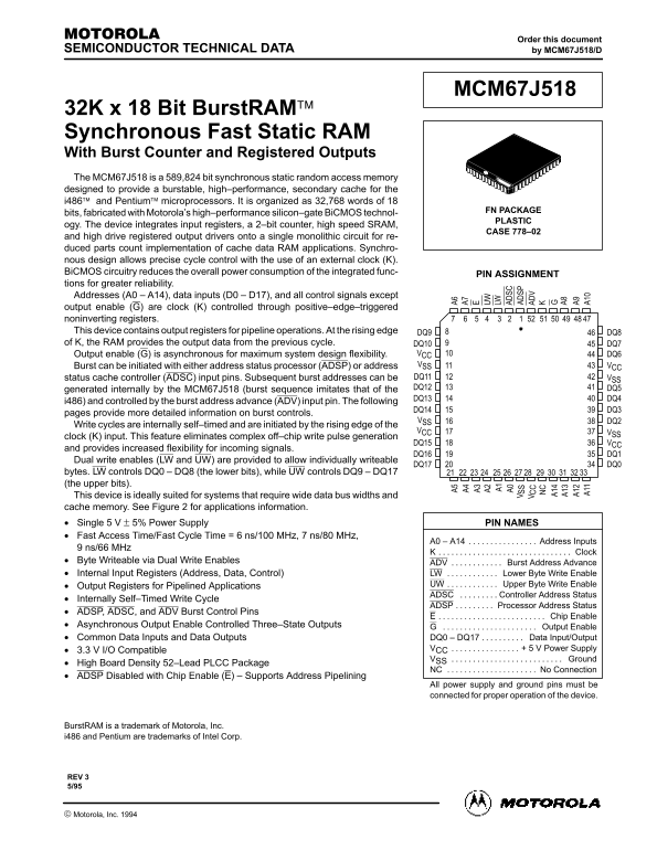
Page 1 Text Content
Order this document
SEMICONDUCTOR TECHNICAL DATA by MCM67J518/D
MCM67J518
32K x 18 Bit Burst RAM Synchronous Fast Static RAM With Burst Counter and Registered Outputs The MCM67J518 is a 589,824 bit synchronous static random access memory designed to provide a burstable, high–performance, secondary cache for the i486 and Pentium microprocessors. It is organized as 32,768 words of 18
FN PACKAGE
bits, fabricated with Motorola’s high–performance silicon–gate Bi CMOS technol-
PLASTIC
ogy. The device integrates input registers, a 2–bit counter, high speed SRAM,
CASE 778–02
and high drive registered output drivers onto a single monolithic circuit for re- duced parts count implementation of cache data RAM applications. Synchro- nous design allows precise cycle control with the use of an external clock (K). Bi CMOS circuitry reduces the overall power consumption of the integrated func-
PIN ASSIGNMENT
tions for greater reliability. Addresses (A0 – A14), data inputs (D0 – D17), and all control signals except output enable (G) are clock (K) controlled through positive–edge–triggered noninverting registers. This device contains output registers for pipeline operations. At the rising edge 8DQ9 DQ8 of K, the RAM provides the output data from the previous cycle. DQ10 DQ7
Output enable (G) is asynchronous for maximum system design flexibility. VCC DQ6 Burst can be initiated with either address status processor (ADSP) or address VSS VCC status cache controller (ADSC) input pins. Subsequent burst addresses can be DQ11 VSS DQ12 DQ5
generated internally by the MCM67J518 (burst sequence imitates that of the
DQ13 DQ4
i486) and controlled by the burst address advance (ADV) input pin. The following
DQ14 DQ3
pages provide more detailed information on burst controls.
VSS DQ2
Write cycles are internally self–timed and are initiated by the rising edge of the
VCC VSS
clock (K) input. This feature eliminates complex off–chip write pulse generation
DQ15 VCC
and provides increased flexibility for incoming signals.
DQ16 A6 DQ1
Dual write enables (LW and UW) are provided to allow individually writeable
DQ17 A7 DQ0
bytes. LW controls DQ0 – DQ8 (the lower bits), while UW controls DQ9 – DQ17
(the upper bits).
This device is ideally suited for systems that require wide data bus widths and
A1 LW
cache memory. See Figure 2 for applications information. SC
SA5 AD SP
Single 5 V ± 5% Power Supply PIN NAMES
Fast Access Time/Fast Cycle Time = 6 ns/100 MHz, 7 ns/80 MHz,
CA4 A0 – A14 Address Inputs. . . . . . . . . . . . . . . .
9 ns/66 MHz
Clock. . . . . . . . . . . . . . . . . . . . . . . . . . . . . . . A1 GAD
Byte Writeable via Dual Write Enables ADV Burst Address Advance. . . . . . . . . . . .
Internal Input Registers (Address, Data, Control) LW Lower Byte Write Enable. . . . . . . . . . . .
Output Registers for Pipelined Applications UW Upper Byte Write Enable. . . . . . . . . . . .
ADSC Controller Address Status. . . . . . . . .
Internally Self–Timed Write Cycle
ADSP Processor Address Status. . . . . . . . .
ADSP, ADSC, and ADV Burst Control Pins
Chip Enable. . . . . . . . . . . . . . . . . . . . . . . . .
Asynchronous Output Enable Controlled Three–State Outputs Output Enable. . . . . . . . . . . . . . . . . . . . . . Common Data Inputs and Data Outputs DQ0 – DQ17 Data Input/Output. . . . . . . . . .
3.3 V I/O Compatible VCC 5 V Power Supply. . . . . . . . . . . . . . . . VSS Ground. . . . . . . . . . . . . . . . . . . . . . . . . .
High Board Density 52–Lead PLCC Package
NC No Connection. . . . . . . . . . . . . . . . . . . . .
ADSP Disabled with Chip Enable (E) – Supports Address Pipelining
All power supply and ground pins must be connected for proper operation of the device.
Burst RAM is a trademark of Motorola, Inc. i486 and Pentium are trademarks of Intel Corp.
REV 3 5/95
MOTOROLA FAST SRAM Motorola, Inc. 1994 MCM67J518
Page Summary Contents For Motorola MCM67J518 Data Sheet/Manual
Manual Details
| Brand | Motorola |
|---|---|
| Pages | 12 |
| File Size | 218.57 KB |
| Published | June 05, 2026 |
Enter the captcha to get the download link:

Frequently Asked Questions
What is the purpose of the MCM67J518 device?
It is a synchronous static random access memory designed to serve as a high-performance, burstable secondary cache for i486 and Pentium microprocessors.
How do I initiate a memory write cycle?
Write cycles are internally self-timed, initiated by the rising edge of the clock (K) input.
Are there separate controls for writing upper and lower bytes?
Yes. LW controls DQ0–DQ8 (lower bits), while UW controls DQ9–DQ17 (upper bits).
What is required for standard operation?
All power supply and ground pins must be connected for proper device operation.