MOTOROLA MC12053A Data Sheet/Manual
Summary
The MC12053A is a super low power dual modulus prescaler semiconductor component, designed for precise RF/IF frequency division. Utilizing specialized Bipolar MOSAIC technology, this device offers selectable divide ratios across two operating modes while maintaining extremely low power consumption and incorporating a stand-by feature to minimize current drain. This technical manual provides electrical characteristics, detailed operational data, logic diagrams, and application graphs necessary for embedding engineers and semiconductor designers who require reliable, high-efficiency frequency synthesis solutions into their custom circuits.
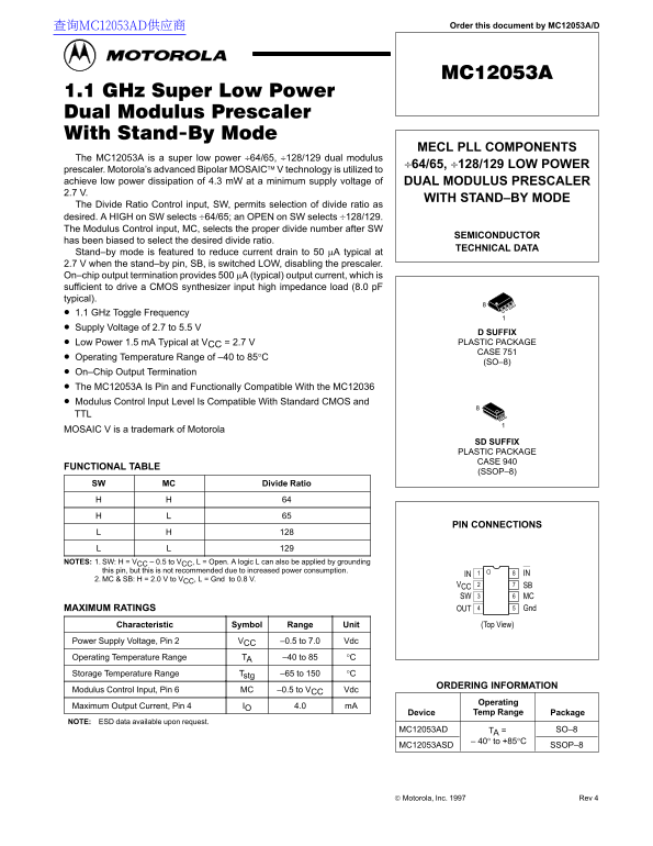
Page 1 Text Content
查询MC12053AD供应商 Order this document by MC12053A/D
MECL PLL COMPONENTS
The MC12053A is a super low power ÷64/65, ÷128/129 dual modulus
÷64/65, ÷128/129 LOW POWER
prescaler. Motorola’s advanced Bipolar MOSAIC V technology is utilized to achieve low power dissipation of 4.3 m W at a minimum supply voltage of DUAL MODULUS PRESCALER 2.7 V.
WITH STAND–BY MODE
The Divide Ratio Control input, SW, permits selection of divide ratio as desired. A HIGH on SW selects ÷64/65; an OPEN on SW selects ÷128/129. The Modulus Control input, MC, selects the proper divide number after SW
SEMICONDUCTOR
has been biased to select the desired divide ratio.
TECHNICAL DATA
Stand–by mode is featured to reduce current drain to 50 µA typical at 2.7 V when the stand–by pin, SB, is switched LOW, disabling the prescaler. On–chip output termination provides 500 µA (typical) output current, which is sufficient to drive a CMOS synthesizer input high impedance load (8.0 p F typical). 1.1 GHz Toggle Frequency Supply Voltage of 2.7 to 5.5 V
D SUFFIX Low Power 1.5 m A Typical at VCC = 2.7 V PLASTIC PACKAGE CASE 751
Operating Temperature Range of –40 to 85°C
(SO–8)
On–Chip Output Termination The MC12053A Is Pin and Functionally Compatible With the MC12036 Modulus Control Input Level Is Compatible With Standard CMOS and TTL MOSAIC V is a trademark of Motorola
SD SUFFIX PLASTIC PACKAGE CASE 940
FUNCTIONAL TABLE
(SSOP–8)
SW MC Divide Ratio
PIN CONNECTIONS
NOTES: 1. SW: H = VCC – 0.5 to VCC, L = Open. A logic L can also be applied by grounding
this pin, but this is not recommended due to increased power consumption.
8IN IN
2. MC & SB: H = 2.0 V to VCC, L = Gnd to 0.8 V.
VCC SB SW MC
MAXIMUM RATINGS OUT Gnd
Characteristic Symbol Range Unit (Top View)
Power Supply Voltage, Pin 2 VCC –0.5 to 7.0 Vdc Operating Temperature Range TA –40 to 85 °C Storage Temperature Range Tstg –65 to 150 °C
ORDERING INFORMATION
Modulus Control Input, Pin 6 MC –0.5 to VCC Vdc
Operating
Maximum Output Current, Pin 4 IO 4.0 m A
Device Temp Range Package
NOTE: ESD data available upon request.
MC12053AD TA = SO–8
40° to +85°C
MC12053ASD SSOP–8
Motorola, Inc. 1997 Rev 4
Page Summary Contents For MOTOROLA MC12053A Data Sheet/Manual
Manual Details
| Brand | Motorola |
|---|---|
| Pages | 7 |
| File Size | 92.61 KB |
| Published | May 30, 2026 |
Enter the captcha to get the download link:

Frequently Asked Questions
How is the divide ratio selected on the MC12053A?
The Divide Ratio Control input (SW) selects the ratio: HIGH selects ÷64/65, and an OPEN circuit selects ÷128/129.
What current drain is achieved in standby mode?
By switching the stand–by pin (SB) LOW, the device can reduce current drain to 50 μA typical at 2.7 V.
Is this component compatible with older parts?
Yes, the MC12053A is pin and functionally compatible with the MC12036.
What is the operating temperature range?
The specified operating temperature range for the module is from –40 to 85°C.