Motorola MC10E167 MC100E167 Data Manual
Summary
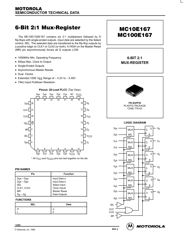
This datasheet provides comprehensive specifications for the MC10E/MC100E167 logic IC, defining its function as a dual-clock multiplexer register containing six 2:1 muxes and D flip-flops. The manual covers crucial electrical parameters, operational high-speed characteristics (up to 1400 MHz), detailed pinouts, timing diagrams, and package dimensions. It is essential reading for hardware engineers and electronics designers who require reliable, high-performance components operating under extended temperature ranges.
Page 1 Text Content
SEMICONDUCTOR TECHNICAL DATA
The MC10E/100E167 contains six 2:1 multiplexers followed by D flip-flops with single-ended outputs. Input data are selected by the Select control, SEL. The selected data are transferred to the flip-flop outputs by a positive edge on CLK1 or CLK2 (or both). A HIGH on the Master Reset (MR) pin asynchronously forces all Q outputs LOW.
1000MHz Min. Operating Frequency 6-BIT 2:1 800ps Max. Clock to Output
MUX-REGISTER
Single-Ended Outputs Asynchronous Master Resets Dual Clocks Extended 100E VEE Range of – 4.2V to – 5.46V 75kΩ Input Pulldown Resistors
Pinout: 28-Lead PLCC (Top View)
VCCONCD3a D3b D4a D4b D5a
D5b Q5 FN SUFFIX PLASTIC PACKAGE CASE 776-02
CLK1 Q4
CLK2 VCC
VEE Q3 LOGIC DIAGRAM
MR Q2 MUX
D0b SEL
SEL VCCO
D0a Q1 MUX
D1b SEL
D0b D1a D1b D2a D2b VCCO Q0 Q2
* All VCC and VCCO pins are tied together on the die.
D2b SEL
PIN NAMES
D3b SEL
Pin Function
D0a D5a Input Data a D4a
D0b D5b Input Data b SEL Select Input SEL
CLK1, CLK2 Clock Inputs
MR Master Reset D5a
Q0 Q5 Data Outputs
D5b SEL
FUNCTIONS
SEL Data SEL
CLK1 CLK2
2–1 REV 2 Motorola, Inc. 1996
Page Summary Contents For Motorola MC10E167 MC100E167 Data Manual
Manual Details
| Brand | Motorola |
|---|---|
| Pages | 5 |
| File Size | 66.93 KB |
| Published | May 30, 2026 |
Enter the captcha to get the download link:

Frequently Asked Questions
What is the minimum operating frequency for this device?
The minimum operating frequency (f Min.) for the MC10E/100E167 is 150 μA, although the manual lists multiple frequencies (e.g., 1400 MHz typical). Please refer to the datasheet's 'Operating Frequency' table section for precise operational limits.
How can I ensure data integrity when using this device?
The device features asynchronous Master Reset (MR), which asynchronously forces all Q outputs LOW, maintaining clean state management during resets.