Motorola MC10E112 MC100E112 Data Manual
Summary
This IC is a high-speed quad driver component designed for Electrically Charged Logic (ECL) applications. It functions primarily as a memory address fan-out or clock driver, offering multiple outputs while maintaining controlled skew performance. This technical manual provides comprehensive specifications, including Detailed DC/AC operating characteristics, pin configurations, and connection guidelines crucial for system integration. It is essential documentation for electrical engineers and hardware designers utilizing high-speed digital logic circuits in embedded systems.
Page 1 Text Content
查询MC100E112供应商 SEMICONDUCTOR TECHNICAL DATA
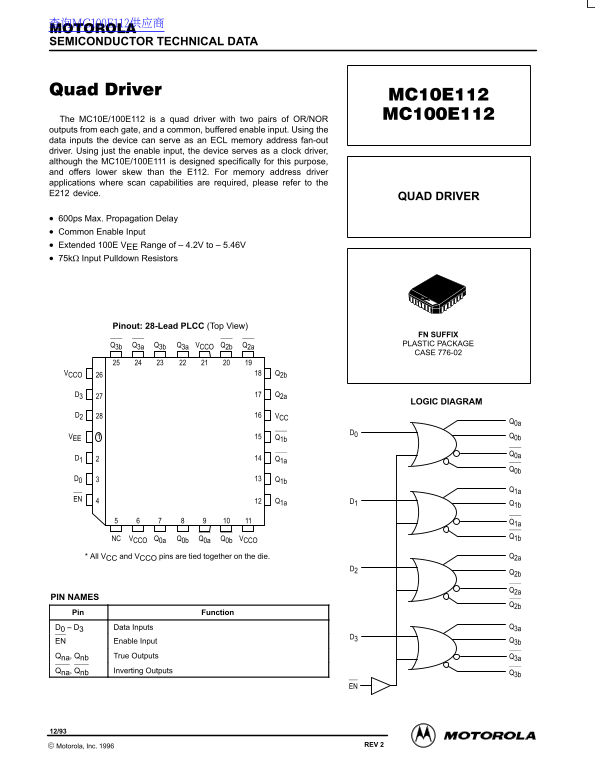
The MC10E/100E112 is a quad driver with two pairs of OR/NOR outputs from each gate, and a common, buffered enable input. Using the data inputs the device can serve as an ECL memory address fan-out driver. Using just the enable input, the device serves as a clock driver, although the MC10E/100E111 is designed specifically for this purpose, and offers lower skew than the E112. For memory address driver applications where scan capabilities are required, please refer to the E212 device.
QUAD DRIVER
600ps Max. Propagation Delay Common Enable Input Extended 100E VEE Range of – 4.2V to – 5.46V 75kΩ Input Pulldown Resistors
Pinout: 28-Lead PLCC (Top View)
FN SUFFIX Q3b Q3a Q3b Q3a VCCO Q2b Q2a PLASTIC PACKAGE CASE 776-02
VCCO Q2b
LOGIC DIAGRAM
D2 VCC
VEE Q1b Q0b
EN Q1a
NC VCCO Q0a Q0b Q0a Q0b VCCO
* All VCC and VCCO pins are tied together on the die. Q2a
PIN NAMES
Pin Function
D0 – D3 Data Inputs Q3a
EN Enable Input Q3b
Qna, Qnb True Outputs Q3a
Qna, Qnb Inverting Outputs
2–1 REV 2 Motorola, Inc. 1996
Page Summary Contents For Motorola MC10E112 MC100E112 Data Manual
Manual Details
| Brand | Motorola |
|---|---|
| Pages | 4 |
| File Size | 100.95 KB |
| Published | May 31, 2026 |
Enter the captcha to get the download link:

Frequently Asked Questions
What alternative device should I use if my memory application requires scan capabilities?
For memory address driver applications requiring scan capabilities, please refer to the E212 device.
What is the maximum propagation delay for the MC10E/100E112?
The maximum propagation delay (tD and tH) is 600ps at room temperature.
What specific task can this quad driver perform besides clock driving?
Using its data inputs, the device can function as an ECL memory address fan-out driver.
How wide is the extended voltage range supported by this driver?
It supports an extended 100E V Range of – 4.2V to – 5.46V.