Motorola MC10E155 MC100E155 Data Manual
Summary
Optimize your digital circuit design with the high-precision MC10E/MC100E155 integrated circuit. This component offers advanced data signal management through multiplexers and latches, ensuring controlled, reliable output in embedded systems. The comprehensive manual serves as a technical reference for hardware engineers and electronics designers, providing detailed pinouts, electrical characteristics, timing diagrams, operational parameters, and application guides necessary for seamless integration into complex logic and switching circuits.
Page 1 Text Content
SEMICONDUCTOR TECHNICAL DATA
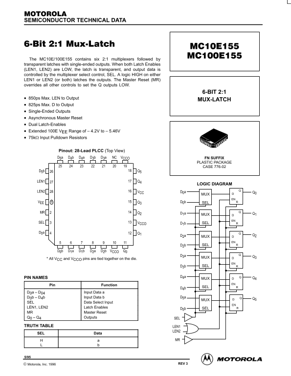
The MC10E/100E155 contains six 2:1 multiplexers followed by transparent latches with single-ended outputs. When both Latch Enables (LEN1, LEN2) are LOW, the latch is transparent, and output data is controlled by the multiplexer select control, SEL. A logic HIGH on either LEN1 or LEN2 (or both) latches the outputs. The Master Reset (MR) overrides all other controls to set the Q outputs LOW.
6-BIT 2:1
850ps Max. LEN to Output
MUX-LATCH
825ps Max. D to Output Single-Ended Outputs Asynchronous Master Reset Dual Latch-Enables Extended 100E VEE Range of – 4.2V to – 5.46V 75kΩ Input Pulldown Resistors
Pinout: 28-Lead PLCC (Top View)
VCCONCD3a D3b D4a D4b D5a FN SUFFIX
PLASTIC PACKAGE CASE 776-02
LEN1 Q4
LOGIC DIAGRAM
LEN2 VCC D0a Q0
VEE Q3 D0b SEL
MR Q2 D1a
MUX Q1
SEL VCCO D1b SEL
D2b SEL
D0b D1a D1b D2a D2b VCCO Q0
MUX Q3
* All VCC and VCCO pins are tied together on the die.
D3b SEL
PIN NAMES D4a
MUX Q4
Pin Function
D0a D04 Input Data a
D0b D4b Input Data b D5a
SEL Data Select Input
LEN1, LEN2 Latch Enables
D5b SEL
MR Master Reset Q0 Q4 Outputs SEL
TRUTH TABLE LEN1
SEL Data
2–1 REV 3 Motorola, Inc. 1996
Page Summary Contents For Motorola MC10E155 MC100E155 Data Manual
Manual Details
| Brand | Motorola |
|---|---|
| Pages | 5 |
| File Size | 66.56 KB |
| Published | May 27, 2026 |
Enter the captcha to get the download link:

Frequently Asked Questions
What controls the device's output outputs?
The outputs are controlled by Latch Enables (LEN1, LEN2), which must be LOW for transparency, and the SEL Data Select input determines the data source.
Are these chips safe for surgical implant applications?
No. Motorola warns that products are not authorized for use in systems intended for surgical implants or life support applications.
What type of physical package is supplied with this IC?
The chip is housed in a 28-Lead PLCC (Plastic Package) with case number 776–02.