Motorola MC10E116 MC100E116 Data Manual
Summary
Engineered for high-speed data transmission, the MC10E116/MC100E116 is a robust quint differential line receiver featuring emitter-follower outputs and excellent common-mode noise rejection. Ideal for advanced twisted pair ECL signaling applications, it includes optimized dedicated supplies and clamp circuitry ensuring optimal stability. This technical summary provides comprehensive documentation, including detailed pinouts, DC characteristics, AC timing parameters, and operational guidelines necessary for electrical engineers designing specialized communication systems.
Page 1 Text Content
查询MC100E116供应商 SEMICONDUCTOR TECHNICAL DATA
The MC10E/100E116 is a quint differential line receiver with emitter-follower outputs. An internally generated reference supply (VBB) is available for single-ended reception.
500ps Max. Propagation Delay
QUINT DIFFERENTIAL
VBB Supply Output
LINE RECEIVER
Dedicated VCCO Pin for Each Receiver Extended 100E VEE Range of – 4.2V to – 5.46V 75kΩ Input Pulldown Resistors
Active current sources plus a deep collector feature of the MOSAIC III process provide the receivers with excellent common-mode noise rejection. Each receiver has a dedicated VCCO supply lead, providing optimum symmetry and stability. The receiver design features clamp circuitry to cause a defined state if both the inverting and non-inverting inputs are left open; in this case the Q output goes LOW, while the Q output goes HIGH. This feature makes the
device ideal for twisted pair applications. FN SUFFIX PLASTIC PACKAGE
If both inverting and non-inverting inputs are at an equal potential of
CASE 776-02
–2.5V, the receiver does not go to a defined state, but rather current-shares in normal differential amplifier fashion, producing output voltage levels midway between HIGH and LOW, or the device may even oscillate. The device VBB output is intended for use as a reference voltage for single-ended reception of ECL signals to that device only. When using for this purpose, it is recommended that VBB is decoupled to VCC via a 0.01µF capacitor. Please refer to the interface section of the design guide for information on using the E116 in specialized applications. The E116 features input pull-down resistors, as does the rest of the ECLin PS family. For applications which require bandwidths greater than that of the E116, the E416 device may be of interest.
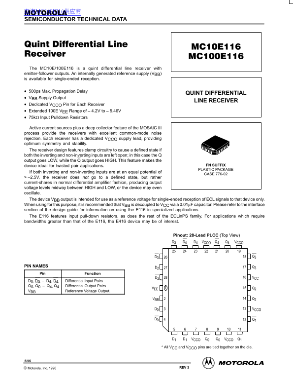
Pinout: 28-Lead PLCC (Top View) D3 D4 D4 VCCO Q4 Q4 VCCO
PIN NAMES Q3
Pin Function
D2 VCC
D0, D0 D4, D4 Differential Input Pairs Q0, Q0 Q4, Q4 Differential Output Pairs
VEE Q2
VBB Reference Voltage Output.
VBB Q2
D0 VCCO
D1 VCCOD1 Q1VCCOQ0Q0
* All VCC and VCCO pins are tied together on the die.
2–1 REV 3 Motorola, Inc. 1996
Page Summary Contents For Motorola MC10E116 MC100E116 Data Manual
Manual Details
| Brand | Motorola |
|---|---|
| Pages | 4 |
| File Size | 109.23 KB |
| Published | May 30, 2026 |
Enter the captcha to get the download link:
