# A B C D E F G H I J K L M N O P Q R S T U V W X Y Z

MOTOROLA 33981 Data Manual

Summary

The 33981 is a versatile, self-protected high-side switch IC designed for modern power management applications. Featuring an extremely low 4.0 mΩ $R_{DS(ON)}$ and PWM control up to 60 kHz, it effectively replaces traditional electromechanical relays and fuses. This technical guide provides comprehensive details on its architecture, including terminal definitions, self-recovery features, and protection mechanisms (such as overcurrent monitoring and undervoltage shutdown). It is essential reading for electrical engineers and power designers working with high inrush current loads, motors, or various resistive/inductive systems requiring robust switching performance.
📄 Preview PAGE OF 24

Page 1 Text Content

re sc le ic to r,

Freescale Semiconductor, Inc.

MOTOROLA Document order number: MC33981

Rev 2.0, 10/2004

SEMICONDUCTOR TECHNICAL DATA

Preliminary Information

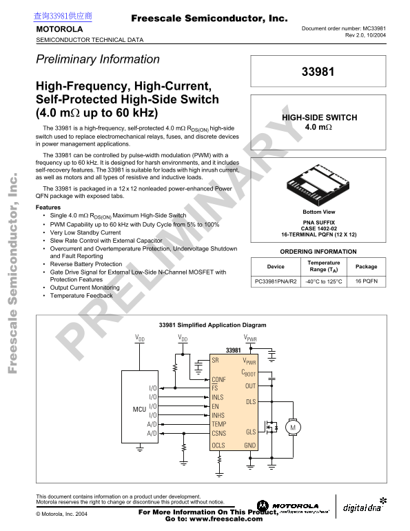
High-Frequency, High-Current, Self-Protected High-Side Switch (4.0 mΩ up to 60 k Hz)

HIGH-SIDE SWITCH The 33981 is a high-frequency, self-protected 4.0 mΩ RDS(ON) high-side 4.0 mΩ

switch used to replace electromechanical relays, fuses, and discrete devices in power management applications. The 33981 can be controlled by pulse-width modulation (PWM) with a frequency up to 60 k Hz. It is designed for harsh environments, and it includes self-recovery features. The 33981 is suitable for loads with high inrush current, as well as motors and all types of resistive and inductive loads. The 33981 is packaged in a 12 nonleaded power-enhanced Power QFN package with exposed tabs. Features

Bottom View

Single 4.0 mΩ RDS(ON) Maximum High-Side Switch

PNA SUFFIX

PWM Capability up to 60 k Hz with Duty Cycle from 5% to 100%

SCALE 1:1 CASE 1402-02

Very Low Standby Current

16-TERMINAL PQFN (12 X 12)

Slew Rate Control with External Capacitor Overcurrent and Overtemperature Protection, Undervoltage Shutdown

ORDERING INFORMATION

and Fault Reporting

Temperature

Reverse Battery Protection

Device Package

Range (TA)

Gate Drive Signal for External Low-Side N-Channel MOSFET with Protection Features

PC33981PNA/R2 -40°C to 125°C 16 PQFN

Output Current Monitoring Temperature Feedback

Simplified Application Diagram

33981 Simplified Application Diagram

VPWRVDDVDD

SR VPWR

CBOOT

I/O FS

I/O INLS

I/O EN MCU I/O INHS

A/D TEMP

A/D CSNS GLS

GNDOCLS

This document contains information on a product under development. Motorola reserves the right to change or discontinue this product without notice.

For More Information On This Product,

© Motorola, Inc. 2004

Go to: www.freescale.com

Page Summary Contents For MOTOROLA 33981 Data Manual

Page 1 re sc le ic to r, Freescale Semiconductor, Inc. MOTOROLA Document order number: MC33981 Rev 2.0, 10/2004 SEMICONDUCTOR TECHNICAL DATA Preliminary Information High-Frequency, High-Current, Self-Protect...
Page 2 re sc le ic to r, Freescale Semiconductor, Inc. Undervoltage Detection Temperature Feedback CBOOTBootstrap Supply Gate Driver Slew Rate Control EN Current Protection Logic INHS OUT Current Recopy Over...
Page 3 re sc le ic to r, Freescale Semiconductor, Inc. Transparent Top View of Package CSNS TEMP EN INHS FS INLS VPWR CONF OCLS DLS GLS SR CBOOT TERMINAL DEFINITIONS Functional descriptions of some of these ...
Page 4 re sc le ic to r, Freescale Semiconductor, Inc. TERMINAL DEFINITIONS (continued) Functional descriptions of some of these terminals can be found in the System/Application Information section beginning...
Page 5 re sc le ic to r, Freescale Semiconductor, Inc. MAXIMUM RATINGS All voltages are with respect to ground unless otherwise noted. Rating Symbol Value Unit ELECTRICAL RATINGS Power Supply Voltage VPWR St...
Page 6 re sc le ic to r, Freescale Semiconductor, Inc. STATIC ELECTRICAL CHARACTERISTICS Characteristics noted under conditions 4.5 VDD 5.5 V, 6.0 VPWR V, -40°C TJ 150°C unless otherwise noted. Typical value...
Page 7 re sc le ic to r, Freescale Semiconductor, Inc. STATIC ELECTRICAL CHARACTERISTICS (continued) Characteristics noted under conditions 4.5 VDD 5.5 V, 6.0 VPWR V, -40°C TJ 150°C unless otherwise noted. T...
Page 8 re sc le ic to r, Freescale Semiconductor, Inc. DYNAMIC ELECTRICAL CHARACTERISTICS Characteristics noted under conditions 4.5 VDD 5.5 V, 6.0 VPWR V, -40°C TJ 150°C unless otherwise noted. Typical valu...
Page 9 re sc le ic to r, Freescale Semiconductor, Inc. Table 1. Functional Truth Table in Normal Mode Condition CONF INHS INLS OUT GLS FS EN Comments Sleep Device is in Sleep mode. The OUT and low-side gate ...
Page 10 re sc le ic to r, Freescale Semiconductor, Inc. Timing Diagram VPWR - 0.5 V t DLY(ON) t DLY(OFF) Figure 2. Time Delays MOTOROLA ANALOG INTEGRATED CIRCUIT DEVICE DATA For More Information On This Produ...
Page 11 re sc le ic to r, Freescale Semiconductor, Inc. Functional Diagrams INHS High Side ON High Side OFF Low Side ON Thermal Shutdown on OUT Thermal Shutdown on OUTThermal Shutdown on OUT Thermal Shutdown ...
Page 12 re sc le ic to r, Freescale Semiconductor, Inc. INHS High Side ON High Side OFF Low Side ON Thermal Shutdown on Bootstrap Circuit or on Low-Side Gate Drive Thermal Shutdown Thermal Shutdown Thermal Sh...
Page 13 re sc le ic to r, Freescale Semiconductor, Inc. µs Min Overload on Low Side Low Side OFF Overload on Low Side Overload on Low Side Overload on Low Side VDS_LS = VOCLS VDS_LS Case 1: Overload Removed F...
Page 14 re sc le ic to r, Freescale Semiconductor, Inc. µs Min Overcurrent on High Side Overcurrent on High Side Overcurrent on High Side Overcurrent on High Side IOCH Fault Removed Figure 7. Overcurrent on O...
Page 15 re sc le ic to r, Freescale Semiconductor, Inc. µs After High Side ON High Side OFF Figure 9. Normal Mode. Independent High Side and Low Side Iout IOUT Figure 10. High-Side Overcurrent MOTOROLA ANALOG...
Page 16 re sc le ic to r, Freescale Semiconductor, Inc. Recirculation in Low Side Current in Motor Figure 11. Cross-Conduction with Low Side Overtemperature Figure 12. Overtemperature on OUT MOTOROLA ANALOG I...
Page 17 re sc le ic to r, Freescale Semiconductor, Inc. Overtemperature Figure 13. Overtemperature on Bootstrap Circuit or on Low-Side Gate Drive Figure 14. Maximum Operating Frequency for SR Capacitor of 4.7...
Page 18 re sc le ic to r, Freescale Semiconductor, Inc. Electrical Performance Curves Ip r(s (S LE le ep EP )(µ A) Rd s O S( (m ) ( hm Temperature (°C) Temp (°C) Figure 15. RDS(ON) versus Temperature Vpwr(V) ...
Page 19 re sc le ic to r, Freescale Semiconductor, Inc. SYSTEM/APPLICATION INFORMATION INTRODUCTION The 33981 is a high-frequency self-protected silicon 4.0 mΩ The 33981 is suitable for loads with high inrush...
Page 20 re sc le ic to r, Freescale Semiconductor, Inc. Configuration Thermal Feedback The CONF terminal manages the cross-conduction between The 33981 has an analog feedback output (TEMP terminal) the intern...
Page 21 re sc le ic to r, Freescale Semiconductor, Inc. APPLICATIONS Figure 18 shows a typical application for the 33981. A brush DC motor is connected to the output. A low-side gate driver is used for the fr...
Page 22 re sc le ic to r, Freescale Semiconductor, Inc. PACKAGE DIMENSIONS PNA SUFFIX 16-TERMINAL PQFN NONLEADED PACKAGE CASE 1402-02 ISSUE B PIN 1 INDEX AREA 2X C0.1 PIN NUMBER REF. ONLY 0.6 DETAIL G SEATING...
Page 23 re sc le ic to r, Freescale Semiconductor, Inc. NOTES MOTOROLA ANALOG INTEGRATED CIRCUIT DEVICE DATA For More Information On This Product, Go to: www.freescale.com
Page 24 re sc le ic to r, Freescale Semiconductor, Inc. Information in this document is provided solely to enable system and software implementers to use Motorola products. There are no express or implied cop...

Manual Details

Brand Motorola
Pages 24
File Size 381.77 KB
Published May 30, 2026
74 views

Enter the captcha to get the download link:

captcha

Frequently Asked Questions

What is the maximum PWM frequency supported by the 33981 switch?

It can be controlled by Pulse-Width Modulation (PWM) up to a frequency of 60 kHz.

What types of loads are suitable for the 33981 High-Side Switch?

It is suitable for motors, high inrush current applications, and all types of resistive and inductive loads.

What protective features does the device offer?

Key protections include Overcurrent, Overtemperature Protection, Undervoltage Shutdown (UVDS), and self-recovery features.

Does it provide an output signal for monitoring high-side current?

Yes, the CSNS terminal outputs a current proportional to the OUT current which can be monitored externally by a microcontroller (MCU).