Motorola MC10E211 MC100E211 Data Manual
Summary
This low-skew 1:6 clock distribution device is engineered for reliable signal transmission in high-speed, synchronous digital circuits. The manual provides comprehensive technical specifications, covering DC/AC characteristics, signal timing requirements, and operation utilizing eCL or PECL inputs. It includes detailed guidelines for implementing multiplexed clock inputs and synchronous enabling/disabling control, making it an essential resource for electrical engineers designing advanced board-level logic systems.
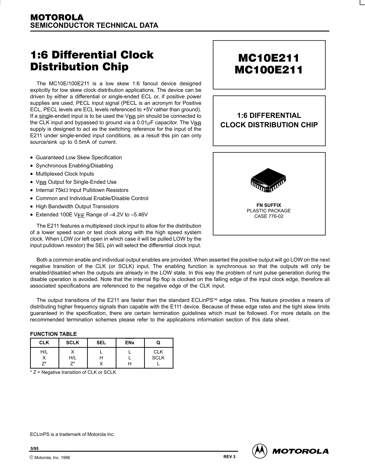
Page 1 Text Content
SEMICONDUCTOR TECHNICAL DATA
The MC10E/100E211 is a low skew 1:6 fanout device designed explicitly for low skew clock distribution applications. The device can be driven by either a differential or single-ended ECL or, if positive power supplies are used, PECL input signal (PECL is an acronym for Positive ECL, PECL levels are ECL levels referenced to +5V rather than ground). If a single-ended input is to be used the VBB pin should be connected to 1:6 DIFFERENTIAL the CLK input and bypassed to ground via a 0.01µF capacitor. The VBB
CLOCK DISTRIBUTION CHIP
supply is designed to act as the switching reference for the input of the E211 under single-ended input conditions, as a result this pin can only source/sink up to 0.5m A of current.
Guaranteed Low Skew Specification Synchronous Enabling/Disabling Multiplexed Clock Inputs VBB Output for Single-Ended Use Internal 75kΩ Input Pulldown Resistors Common and Individual Enable/Disable Control
FN SUFFIX
High Bandwidth Output Transistors
PLASTIC PACKAGE
Extended 100E VEE Range of –4.2V to –5.46V
CASE 776-02
The E211 features a multiplexed clock input to allow for the distribution of a lower speed scan or test clock along with the high speed system clock. When LOW (or left open in which case it will be pulled LOW by the input pulldown resistor) the SEL pin will select the differential clock input.
Both a common enable and individual output enables are provided. When asserted the positive output will go LOW on the next negative transition of the CLK (or SCLK) input. The enabling function is synchronous so that the outputs will only be enabled/disabled when the outputs are already in the LOW state. In this way the problem of runt pulse generation during the disable operation is avoided. Note that the internal flip flop is clocked on the falling edge of the input clock edge, therefore all associated specifications are referenced to the negative edge of the CLK input.
The output transitions of the E211 are faster than the standard ECLin PS edge rates. This feature provides a means of distributing higher frequency signals than capable with the E111 device. Because of these edge rates and the tight skew limits guaranteed in the specification, there are certain termination guidelines which must be followed. For more details on the recommended termination schemes please refer to the applications information section of this data sheet.
FUNCTION TABLE CLK SCLK SEL ENx H/L CLK
H/L SCLK
Z* Z* * Z = Negative transition of CLK or SCLK
ECLin PS is a trademark of Motorola Inc.
2–1 REV 3 Motorola, Inc. 1996
Page Summary Contents For Motorola MC10E211 MC100E211 Data Manual
Manual Details
| Brand | Motorola |
|---|---|
| Pages | 8 |
| File Size | 77.85 KB |
| Published | July 16, 2026 |
Enter the captcha to get the download link:

Frequently Asked Questions
How should I configure a single-ended input connection?
The V pin must be connected to the 1:6 DIFFERENTIAL BB the CLK input and bypassed to ground using a 0.01µF capacitor.
What is the purpose of the SEL pin on this E211 device?
When the SEL pin is LOW, it selects the differential clock input for multiplexed clock distribution.
What are the guaranteed limits for within-device skew?
The guaranteed within-device skew is between 50 and 75 ps.
Can this chip be used in implantable medical devices?
No. Motorola products are not authorized for use as components in systems intended for surgical implants or life support applications.