Motorola MC10E104 MC100E104 Data Manual
Summary
The MC10E/MC100E104 is a high-performance quint 2-input AND/NAND logic gate featuring integrated OR/NOR function outputs and extended operating voltage capabilities (-4.2V to -5.46V). This comprehensive manual serves as the definitive resource for digital circuit designers and electronics engineers, providing complete technical specifications. It details all electrical characteristics (DC/AC), crucial timing parameters (e.g., propagation delay, skew), precise pinouts, package dimensions, and operational guidelines needed for integrating the low-power logic gate into advanced electronic systems.
Page 1 Text Content
查询MC100E104供应商 SEMICONDUCTOR TECHNICAL DATA
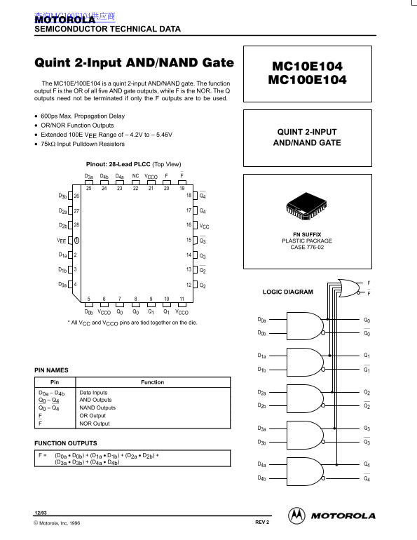
The MC10E/100E104 is a quint 2-input AND/NAND gate. The function output F is the OR of all five AND gate outputs, while F is the NOR. The Q outputs need not be terminated if only the F outputs are to be used.
600ps Max. Propagation Delay OR/NOR Function Outputs
QUINT 2-INPUT
Extended 100E VEE Range of – 4.2V to – 5.46V
75kΩ Input Pulldown Resistors AND/NAND GATE
Pinout: 28-Lead PLCC (Top View)
FFVCCONCD4a D4b D3a
D2b VCC
FN SUFFIX
VEE Q3 PLASTIC PACKAGE
CASE 776-02
LOGIC DIAGRAM
D0b VCCO Q0 Q0 Q1 Q1 VCCO
* All VCC and VCCO pins are tied together on the die.
PIN NAMES D1b Q1
Pin Function
D0a D4b Data Inputs D2a Q2
Q0 Q4 AND Outputs
Q0 Q4 NAND Outputs
OR Output NOR Output
FUNCTION OUTPUTS F = (D0a • D0b) + (D1a • D1b) + (D2a • D2b) + (D3a • D3b) + (D4a • D4b)
2–1 REV 2 Motorola, Inc. 1996
Page Summary Contents For Motorola MC10E104 MC100E104 Data Manual
Manual Details
| Brand | Motorola |
|---|---|
| Pages | 4 |
| File Size | 103.85 KB |
| Published | June 05, 2026 |
Enter the captcha to get the download link:

Frequently Asked Questions
What is the functional difference between the F and NOR outputs?
The F output acts as an OR of all five AND gate outputs; conversely, the dedicated NOR function provides a separate signal.
What extended voltage range does this device support?
It supports an extended 100E V Range spanning from –4.2V to –5.46V.
Can this logic gate be used in sensitive medical or life-support systems?
No, it is not designed for use in surgical implants or any application where failure could cause personal injury or death.
What is the typical maximum propagation delay (D to Q)?
The typical transmission time from D to Q has a maximum reported propagation delay of 600ps.