Fairchild PF5102 N-Channel Switch User's Manual
Summary
This N-Channel Switch is a specialized semiconductor component ideal for low-level analog switching, sample and hold circuits, and chopper stabilized amplifier applications. The comprehensive manual provides crucial technical specifications, including absolute maximum ratings, detailed thermal characteristics, full electrical parameters (on/off state), and small signal data. It serves electronics engineers and designers who require reliable components for precision analog circuit development.
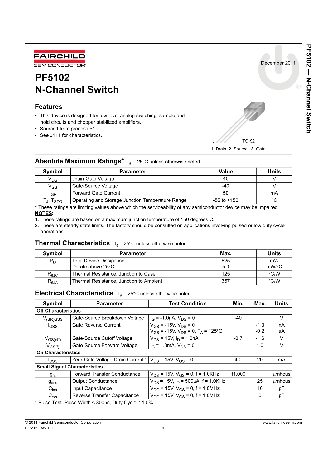
Page 1 Text Content
PF5102 — -C hannel Sw itch
December 2011
PF5102 N-Channel Switch Features This device is designed for low level analog switching, sample and hold circuits and chopper stabilized amplifiers. Sourced from process 51. See J111 for characteristics.
TO-92
1. Drain 2. Source 3. Gate
Absolute Maximum Ratings* Ta = 25°C unless otherwise noted Symbol Parameter Value Units VDG Drain-Gate Voltage
VGS Gate-Source Voltage -40 IGF Forward Gate Current m A
TJ, TSTG Operating and Storage Junction Temperature Range -55 to +150 °C * These ratings are limiting values above which the serviceability of any semiconductor device may be impaired. NOTES: 1. These ratings are based on a maximum junction temperature of 150 degrees C. 2. These are steady state limits. The factory should be consulted on applications involving pulsed or low duty cycle operations.
Thermal Characteristics Ta = 25°C unless otherwise noted Symbol Parameter Max. Units PD Total Device Dissipation m W
Derate above 25°C 5.0 m W/°C RθJC Thermal Resistance, Junction to Case °C/W RθJA Thermal Resistance, Junction to Ambient °C/W
Electrical Characteristics Ta = 25°C unless otherwise noted Symbol Parameter Test Condition Min. Max. Units Off Characteristics V(BR)GSS Gate-Source Breakdown Voltage IG = -1.0μA, VDS = 0 -40
IGSS Gate Reverse Current VGS = -15V, VDS = 0 -1.0 n A
VGS = -15V, VDS = 0, TA = 125°C -0.2 μA
VGS(off) Gate-Source Cutoff Voltage VDS = 15V, ID = 1.0n A -0.7 -1.6 VGS(f) Gate-Source Forward Voltage IG = 1.0m A, VDS = 0 1.0
On Characteristics
IDSS Zero-Gate Voltage Drain Current * VDS = 15V, VGS = 0 4.0 m A
Small Signal Characteristics
gfs Forward Transfer Conductance VDS = 15V, VGS = 0, f = 1.0KHz 11,000 μmhous goss Output Conductance VDS = 15V, ID = 500μA, f = 1.0KHz μmhous Ciss Input Capacitance VDG = 15V, VGS = 0, f = 1.0MHz p F
Crss Reverse Transfer Capacitance VDG = 15V, VGS = 0, f = 1.0MHz p F * Pulse Test: Pulse Width ≤ 300μs, Duty Cycle ≤ 1.0%
© 2011 Fairchild Semiconductor Corporation www.fairchildsemi.com PF5102 Rev. B0
Page Summary Contents For Fairchild PF5102 N-Channel Switch User's Manual
Manual Details
| Brand | Fairchild |
|---|---|
| Pages | 3 |
| File Size | 125.70 KB |
| Published | July 06, 2026 |
Enter the captcha to get the download link:

Frequently Asked Questions
What specific applications is the PF5102 switch designed for?
It is designed for low level analog switching, sample and hold circuits, and chopper stabilized amplifiers.
What is the required method for purchasing genuine components?
You must purchase parts directly from Fairchild or an Authorized Distributor listed on their website.
Can this device be used as a critical component in life support systems?
No, it requires express written approval from Fairchild Semiconductor Corporation before use in such devices.
What is the maximum allowable junction temperature range?
The operating and storage junction temperature range is specified as -55 to +150 °C.