Fairchild PN4117/18/19 N-Channel Switch Data Handbook
Summary
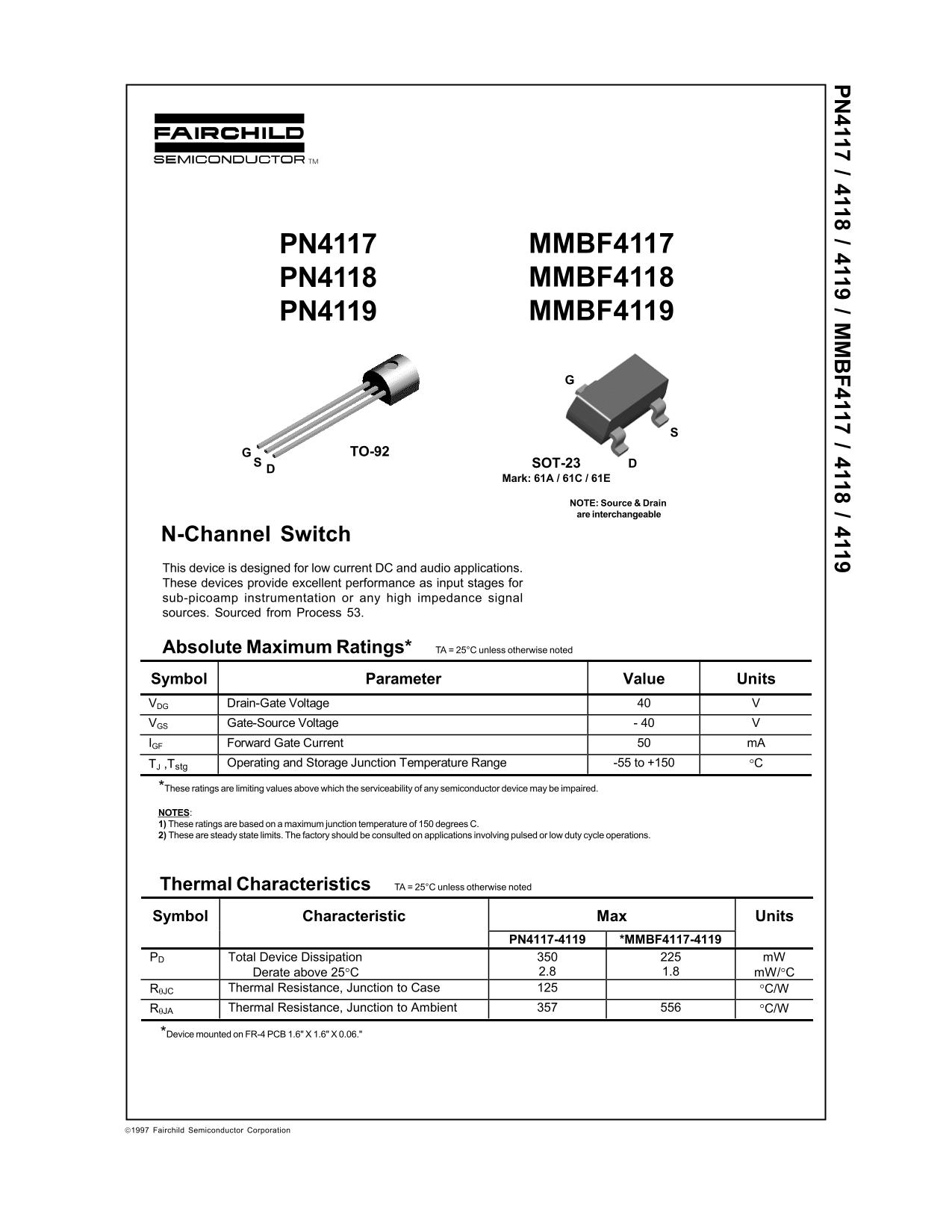
Fairchild Semiconductor PN4117/PN4118/PN4119/MMBF4117/MMBF4118/MMBF4119 N-Channel JFET switch datasheet documenting low-current DC and audio switching devices sourced from Process 53. Designed for sub-picoamp instrumentation input stages and high-impedance signal sources with interchangeable source and drain terminals. Available in TO-92 (PN-series) and SOT-23 (MMBF-series, marks: 61A/61C/61E) packages. Key specs: 40V drain-gate breakdown, -40V gate-source voltage, 50mA forward gate current, gat
Page 1 Text Content
PN4117 MMBF4117 PN4118 MMBF4118 PN4119 MMBF4119
TO-92
SOT-23 Mark: 61A / 61C / 61E NOTE: Source & Drain are interchangeable
N-Channel Switch This device is designed for low current DC and audio applications. These devices provide excellent performance as input stages for sub-picoamp instrumentation or any high impedance signal sources. Sourced from Process 53.
Absolute Maximum Ratings* TA = 25°C unless otherwise noted Symbol Parameter Value Units VDG Drain-Gate Voltage VGS Gate-Source Voltage - 40 IGF Forward Gate Current m A
TJ ,Tstg Operating and Storage Junction Temperature Range -55 to +150 °C
*These ratings are limiting values above which the serviceability of any semiconductor device may be impaired. NOTES: 1) These ratings are based on a maximum junction temperature of 150 degrees C. 2) These are steady state limits. The factory should be consulted on applications involving pulsed or low duty cycle operations.
Thermal Characteristics TA = 25°C unless otherwise noted Symbol Characteristic Max Units
PN4117-4119 *MMBF4117-4119
PD Total Device Dissipation m W
Derate above 25°C 2.8 1.8 m W/°C
RθJC Thermal Resistance, Junction to Case °C/W RθJA Thermal Resistance, Junction to Ambient °C/W
*Device mounted on FR-4 PCB 1.6" X 1.6" X 0.06."
1997 Fairchild Semiconductor Corporation
Page Summary Contents For Fairchild PN4117/18/19 N-Channel Switch Data Handbook
Manual Details
| Brand | Fairchild |
|---|---|
| Pages | 5 |
| File Size | 128.62 KB |
| Published | July 06, 2026 |
Enter the captcha to get the download link:

Frequently Asked Questions
What is the recommended application for this device?
This N-Channel Switch is designed for low current DC and audio applications, providing excellent input stages for high impedance signal sources.
How should I calculate derating for elevated temperatures?
The total device dissipation must be derated (mW/°C) when operating above 25°C. The maximum rating is 350 mW at 25°C.
Are the Source and Drain pins interchangeable?
Yes, the manual notes that Source & Drain are interchangeable for these devices.
What are the typical Transconductance values (f=1.0 kHz)?
The typical range varies by model: PN4117 is 70-210 µmhos; PN4118 is 100-330 µmhos; and PN4119 is not specified in this section.