Fairchild 74VHC00 Quad 2-Input NAND Gate Data Manual
Summary
The 74VHC00 is a high-speed CMOS Quad 2-Input NAND Gate designed for robust digital logic applications. Featuring exceptional noise immunity and low power dissipation (I=2µA), it includes an advanced input protection circuit allowing reliable interfacing across diverse voltage systems, such as battery backups or 3V to 5V setups. This technical manual provides comprehensive specifications, including recommended operating conditions, electrical characteristics, maximum ratings, and multiple package options (SOIC, TSSOP, PDIP). It is essential for hardware engineers and designers requiring a stable, reliable, and high-speed logic solution for complex embedded systems.
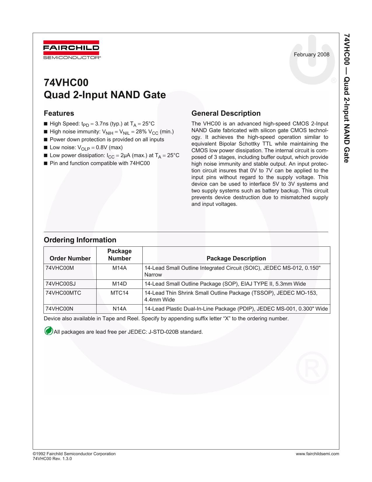
Page 1 Text Content
74V 00 — ad 2-In t N ate
February 2008
74VHC00 Quad 2-Input NAND Gate Features General Description High Speed: t PD = 3.7ns (typ.) at TA = 25°C The VHC00 is an advanced high-speed CMOS 2-Input
High noise immunity: VNIH = VNIL = 28% VCC (min.) NAND Gate fabricated with silicon gate CMOS technol- ogy. It achieves the high-speed operation similar to
Power down protection is provided on all inputs
equivalent Bipolar Schottky TTL while maintaining the
Low noise: VOLP = 0.8V (max)
CMOS low power dissipation. The internal circuit is com-
Low power dissipation: ICC = 2µA (max.) at TA = 25°C
posed of 3 stages, including buffer output, which provide
Pin and function compatible with 74HC00 high noise immunity and stable output. An input protec-
tion circuit insures that 0V to 7V can be applied to the input pins without regard to the supply voltage. This device can be used to interface 5V to 3V systems and two supply systems such as battery backup. This circuit prevents device destruction due to mismatched supply and input voltages.
Ordering Information
Package
Order Number Number Package Description 74VHC00M M14A 14-Lead Small Outline Integrated Circuit (SOIC), JEDEC MS-012, 0.150"
Narrow
74VHC00SJ M14D 14-Lead Small Outline Package (SOP), EIAJ TYPE II, 5.3mm Wide 74VHC00MTC MTC14 14-Lead Thin Shrink Small Outline Package (TSSOP), JEDEC MO-153,
4.4mm Wide
74VHC00N N14A 14-Lead Plastic Dual-In-Line Package (PDIP), JEDEC MS-001, 0.300" Wide Device also available in Tape and Reel. Specify by appending suffix letter “X” to the ordering number.
All packages are lead free per JEDEC: J-STD-020B standard.
©1 992 Fairchild Semiconductor Corporation www.fairchildsemi.com 74V HC00 Rev. 1.3.0
Page Summary Contents For Fairchild 74VHC00 Quad 2-Input NAND Gate Data Manual
Manual Details
| Brand | Fairchild |
|---|---|
| Pages | 10 |
| File Size | 293.28 KB |
| Published | July 06, 2026 |
Enter the captcha to get the download link:

Frequently Asked Questions
What input voltage range can I apply to the pins?
The input protection circuit allows voltages from 0V to 7V, regardless of the supply voltage.
Can this gate connect systems with different supply voltages (e.g., battery backup)?
Yes, it can interface 5V to 3V systems and two separate supply sources.
What is the device's typical high-speed switching time?
The typical rise time (t) at room temperature is 3.7ns.
If I leave an input pin unconnected, what must I do?
Unused inputs must be held either HIGH or LOW; they should not be allowed to float.