Fairchild CD4001BC CD4011BC Quad 2-Input NOR Buffered B Series Gate, Quad 2-Input NAND Buffered B Series Gate - Data Manual
Summary
These low-power CMOS quad logic gates provide core NAND and NOR functionality for robust digital circuit design. The manual is a comprehensive technical resource detailing electrical characteristics, operational parameters, temperature ranges, and multiple packaging options (SOIC, SOP, PDIP). It is essential documentation for electronic engineers and hardware designers needing reliable and standardized integrated circuit components for advanced system development.
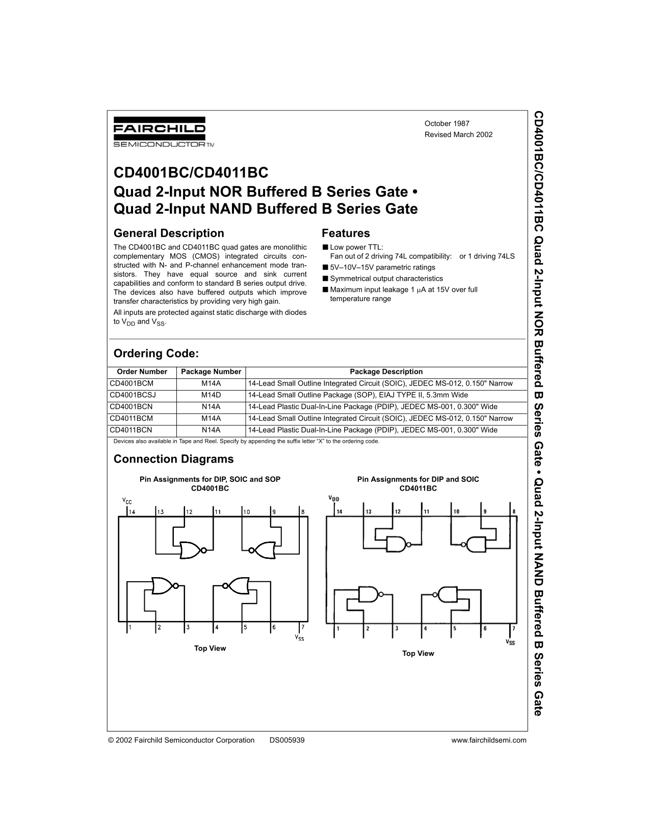
Page 1 Text Content
4001B /C 4011B ad 2-In t N ffered eries G ate • Q ad 2-In t N ffered eries G ate
October 1987 Revised March 2002
CD4001BC/CD4011BC Quad 2-Input NOR Buffered B Series Gate • Quad 2-Input NAND Buffered B Series Gate General Description Features The CD4001BC and CD4011BC quad gates are monolithic ■Low power TTL: complementary MOS (CMOS) integrated circuits con- Fan out of 2 driving 74L compatibility: or 1 driving 74LS structed with N- and P-channel enhancement mode tran-
■5V–10V–15V parametric ratings
sistors. They have equal source and sink current
■Symmetrical output characteristics
capabilities and conform to standard B series output drive.
■Maximum input leakage 1 µA at 15V over full
The devices also have buffered outputs which improve
temperature range
transfer characteristics by providing very high gain. All inputs are protected against static discharge with diodes to VDD and VSS.
Ordering Code: Order Number Package Number Package Description CD4001BCM M14A 14-Lead Small Outline Integrated Circuit (SOIC), JEDEC MS-012, 0.150" Narrow CD4001BCSJ M14D 14-Lead Small Outline Package (SOP), EIAJ TYPE II, 5.3mm Wide CD4001BCN N14A 14-Lead Plastic Dual-In-Line Package (PDIP), JEDEC MS-001, 0.300" Wide CD4011BCM M14A 14-Lead Small Outline Integrated Circuit (SOIC), JEDEC MS-012, 0.150" Narrow CD4011BCN N14A 14-Lead Plastic Dual-In-Line Package (PDIP), JEDEC MS-001, 0.300" Wide Devices also available in Tape and Reel. Specify by appending the suffix letter “X” to the ordering code.
Connection Diagrams Pin Assignments for DIP, SOIC and SOP Pin Assignments for DIP and SOIC
CD4001BC CD4011BC
Top View
Top View
© 2002 Fairchild Semiconductor Corporation DS005939 www.fairchildsemi.com
Page Summary Contents For Fairchild CD4001BC CD4011BC Quad 2-Input NOR Buffered B Series Gate, Quad 2-Input NAND Buffered B Series Gate - Data Manual
Manual Details
| Brand | Fairchild |
|---|---|
| Pages | 9 |
| File Size | 118.03 KB |
| Published | July 06, 2026 |
Enter the captcha to get the download link:

Frequently Asked Questions
What voltage range can this integrated circuit operate within?
The recommended operating range (VDD) is between 3V and 15V.
Are these devices protected against electrical surges during handling?
Yes, all inputs are protected against static discharge with diodes to VDD and VSS.
What warning must I consider regarding critical applications?
Fairchild products are not authorized for use as critical components in life support devices or systems without the express written approval of Fairchild Semiconductor Corporation.
How are these gates packaged and ordered?
They are available in 14-Lead Small Outline (SOIC), Small Outline Package (SOP), and Plastic Dual-In-Line Package (PDIP) formats.