National Semiconductor CD4071BM CD4071BC Quad 2-Input OR Buffered B Series Gate Data Sheet
Summary
Essential components for designing stable digital circuitry, this series features Quad 2-Input OR (CD4071) and AND (CD4081) logic gates. The accompanying manual provides comprehensive technical documentation, detailing the electrical characteristics, operating ratings, and performance specifications across various industrial temperature ranges. It is tailored for electronics engineers and circuit designers seeking reliable, buffered CMOS/TTL compatibility ICs for their professional projects.
Page 1 Text Content
查询CD4071BC供应商
February
-In ffe re rie te -In ffe re rie te
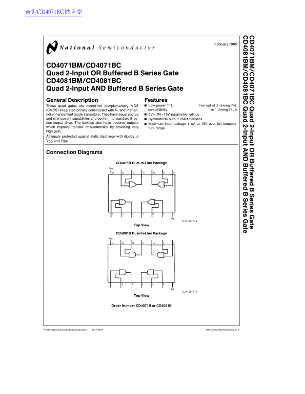
CD4071BM/CD4071BC Quad 2-Input OR Buffered Series Gate CD4081BM/CD4081BC Quad 2-Input AND Buffered Series Gate General Description Features
These quad gates are monolithic complementary MOS Low power TTL Fan out of driving 74L (CMOS) integrated circuits constructed with N- and P-chan- compatibility or driving 74LS
nel enhancement mode transistors. They have equal source 5V–10V–15V parametric ratings and sink current capabilities and conform to standard se- Symmetrical output characteristics ries output drive. The devices also have buffered outputs
Maximum input leakage m A at 15V over full tempera-
which improve transfer characteristics by providing very
ture range
high gain. All inputs protected against static discharge with diodes to VDD and VSS.
Connection Diagrams
CD4071B Dual-In-Line Package
TL/F/5977–3
CD4081B Dual-In-Line Package
TL/F/5977–6
Order Number CD4071B or CD4081B
C1995 National Semiconductor Corporation TL/F/5977 RRD-B30M105/Printed in U. S. A.
Page Summary Contents For National Semiconductor CD4071BM CD4071BC Quad 2-Input OR Buffered B Series Gate Data Sheet
Manual Details
| Brand | National |
|---|---|
| Pages | 8 |
| File Size | 182.59 KB |
| Published | June 17, 2026 |
Enter the captcha to get the download link:

Frequently Asked Questions
What is the primary function of these quad gates?
They are monolithic complementary MOS (CMOS) compatible gates that provide buffered outputs, having either OR or AND logic functions.
What operating temperature ranges are provided for different CD4071/CD4081 versions?
The 'BM' variants have a range of -55°C to 125°C; the 'BC' variants operate between -40°C and 85°C.
How are these devices protected against electrical interference?
All inputs are protected against static discharge using diodes to Vdd and Vs.
What is the recommended operating voltage range for these chips?
The specified operating voltage (Vdd) must be between 3V and 15V.