ST HCF4001B QUAD 2-INPUT NOR GATE Data Sheet
Summary
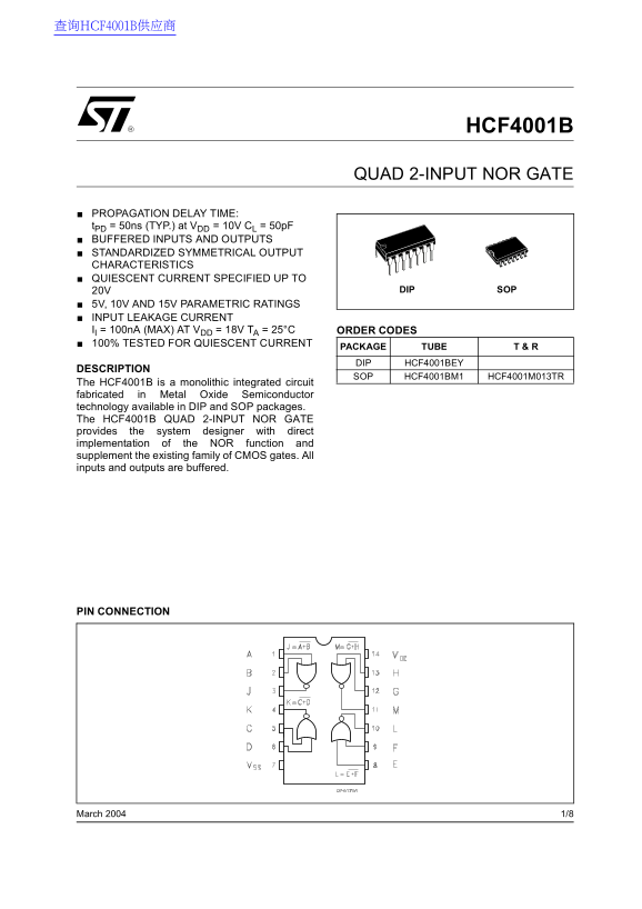
This integrated circuit delivers a buffered QUAD 2-INPUT NOR GATE function, ideal for system designers implementing standard CMOS logic in their electronic designs. The accompanying manual provides comprehensive technical documentation, detailing absolute maximum ratings, DC and dynamic electrical characteristics, pin assignments, and mechanical specifications for DIP, SOP, and Tape & Reel packages. Whether you need reliable high-speed performance or detailed parameter verification, this resource supports design integration across various voltage levels (from 3V to 20V).
Page 1 Text Content
查询HCF4001B供应商
HCF4001B
QUAD 2-INPUT NOR GATE
PROPAGATION DELAY TIME: t PD 50ns (TYP.) at VDD 10V CL 50p F BUFFERED INPUTS AND OUTPUTS STANDARDIZED SYMMETRICAL OUTPUT CHARACTERISTICS QUIESCENT CURRENT SPECIFIED UP TO
20V DIP SOP
5V, 10V AND 15V PARAMETRIC RATINGS INPUT LEAKAGE CURRENT II 100n A (MAX) AT VDD 18V TA 25°C ORDER CODES 100% TESTED FOR QUIESCENT CURRENT
PACKAGE TUBE DIP HCF4001BEY
DESCRIPTION
SOP HCF4001BM1 HCF4001M013TR
The HCF4001B is monolithic integrated circuit fabricated in Metal Oxide Semiconductor technology available in DIP and SOP packages. The HCF4001B QUAD 2-INPUT NOR GATE provides the system designer with direct implementation of the NOR function and supplement the existing family of CMOS gates. All inputs and outputs are buffered.
PIN CONNECTION
1/8March
Page Summary Contents For ST HCF4001B QUAD 2-INPUT NOR GATE Data Sheet
Manual Details
| Brand | QUAD |
|---|---|
| Pages | 8 |
| File Size | 111.10 KB |
| Published | May 27, 2026 |
Enter the captcha to get the download link:
