ST 74LCX02 Low-Voltage CMOS Quad 2-Input NOR Gate with 5V Tolerant Inputs Data Manual
Summary
A high-performance, low-voltage CMOS Quad 2-Input NOR Gate operating reliably between 2.0V and 3.6V. Engineered for modern digital applications, it provides robust functionality, excellent ESD immunity, and guaranteed PCI bus levels while consuming minimal power. This technical manual serves as a comprehensive guide for engineers, providing detailed electrical specifications, timing characteristics (t=4.4ns), absolute maximum ratings, and pin compatibility with the 74 series. It is ideally suited for designing high-speed, low-power digital systems that require integration into complex logic environments.
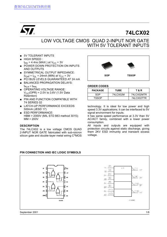
Page 1 Text Content
查询74LCX02MTR供应商
74LCX02
LOW VOLTAGE CMOS QUAD 2-INPUT NOR GATE
WITH 5V TOLERANT INPUTS
5V TOLERANT INPUTS HIGH SPEED : t PD = 4.4ns (MAX.) at VCC = 3V POWER DOWN PROTECTION ON INPUTS AND OUTPUTS SYMMETRICAL OUTPUT IMPEDANCE:
|IOH| = IOL = 24m A (MIN) at VCC = 3V TSSOPSOP
PCI BUS LEVELS GUARANTEED AT 24 m A BALANCED PROPAGATION DELAYS: t PLH ≅ t PHL ORDER CODES OPERATING VOLTAGE RANGE:
PACKAGE TUBE T & R
VCC(OPR) = 2.0V to 3.6V (1.5V Data
SOP 74LCX02M 74LCX02MTR
Retention)
TSSOP 74LCX02TTR
PIN AND FUNCTION COMPATIBLE WITH 74 SERIES 02 LATCH-UP PERFORMANCE EXCEEDS technology. It is ideal for low power and high 500m A (JESD 17) speed 3.3V applications; it can be interfaced to 5V
ESD PERFORMANCE: signal environment for inputs.
HBM > 2000V (MIL STD 883 method 3015); It has same speed performance at 3.3V than 5V MM > 200V AC/ACT family, combined with a lower power
consumption. DESCRIPTION All inputs and outputs are equipped with The 74LCX02 is a low voltage CMOS QUAD protection circuits against static discharge, giving them 2KV ESD immunity and transient excess
2-INPUT NOR GATE fabricated with sub-micron
voltage.
silicon gate and double-layer metal wiring C2MOS
PIN CONNECTION AND IEC LOGIC SYMBOLS
1/8September 2001
Page Summary Contents For ST 74LCX02 Low-Voltage CMOS Quad 2-Input NOR Gate with 5V Tolerant Inputs Data Manual
Manual Details
| Brand | QUAD |
|---|---|
| Pages | 8 |
| File Size | 139.76 KB |
| Published | May 31, 2026 |
Enter the captcha to get the download link:

Frequently Asked Questions
Is this NOR gate compatible with standard 74 series logic?
Yes, it is noted as being PIN and function compatible with the entire 74 series 02 family.
What is the maximum ESD protection level of the component?
The device offers high ESD immunity, which exceeds 2000V according to MIL STD 883 method 3015.
Can this gate handle signals from a standard 5V supply environment?
Yes, it includes features like 5V tolerant inputs and guarantees PCI BUS LEVELS at 24 mA.
What is the recommended operating voltage range (VCC)?
The optimal operating voltage range for stable function is between 2.0V and 3.6V.