FAIRCHILD semiconductor 74LCX00 Low Voltage Quad 2-Input NAND Gate with 5V Tolerant Inputs Data Manual
Summary
The 74LCX00 is a robust low-voltage quad 2-input NAND gate built with advanced CMOS technology, providing high speed and minimal power consumption. Featuring 5V tolerant inputs, it ensures reliable interfacing across various system voltages (2.3V–3.6V). This comprehensive manual details its electrical characteristics, operating limits, multiple package options (SOIC, SOP, TSSOP), and performance specifications for engineers designing reliable digital logic circuits into their systems.
Page 1 Text Content
查询74LCX00供应商
74L 00 L ltag e Q ad 2-In t N ate w ith 5V To leran t In ts
March 1995 Revised March 1999
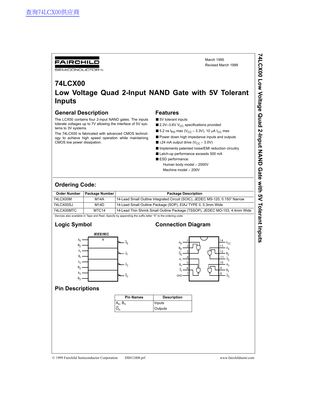
74LCX00 Low Voltage Quad 2-Input NAND Gate with 5V Tolerant Inputs General Description Features The LCX00 contains four 2-input NAND gates. The inputs 5V tolerant inputs tolerate voltages up to 7V allowing the interface of 5V sys- 2.3V–3.6V VCC specifications provided tems to 3V systems.
5.2 ns t PD max (VCC = 3.3V), 10 µA ICC max
The 74LCX00 is fabricated with advanced CMOS technol-
ogy to achieve high speed operation while maintaining Power down high impedance inputs and outputs CMOS low power dissipation. ±24 m A output drive (VCC = 3.0V) Implements patented noise/EMI reduction circuitry Latch-up performance exceeds 500 m A ESD performance: Human body model > 2000V Machine model > 200V
Ordering Code: Order Number Package Number Package Description 74LCX00M M14A 14-Lead Small Outline Integrated Circuit (SOIC), JEDEC MS-120, 0.150” Narrow 74LCX00SJ M14D 14-Lead Small Outline Package (SOP), EIAJ TYPE II, 5.3mm Wide 74LCX00MTC MTC14 14-Lead Thin Shrink Small Outline Package (TSSOP), JEDEC MO-153, 4.4mm Wide Devices also available in Tape and Reel. Specify by appending the suffix letter “X” to the ordering code.
Logic Symbol Connection Diagram
IEEE/IEC
Pin Descriptions
Pin Names Description
An, Bn Inputs On Outputs
© 1999 Fairchild Semiconductor Corporation DS012408.prf www.fairchildsemi.com
Page Summary Contents For FAIRCHILD semiconductor 74LCX00 Low Voltage Quad 2-Input NAND Gate with 5V Tolerant Inputs Data Manual
Manual Details
| Brand | Fairchild |
|---|---|
| Pages | 7 |
| File Size | 83.16 KB |
| Published | July 06, 2026 |
Enter the captcha to get the download link:

Frequently Asked Questions
Can this chip interface with both 5V and standard low voltage systems?
Yes, it features 5V tolerant inputs, allowing interfacing of 5V systems with 2.3V–3.6V Vcc systems.
What are the required conditions for operational temperature?
The recommended free-air operating temperature range is -40°C to 85°C degrees Celsius.
If I set this chip up, what should I do with unused input pins?
Unused inputs must be held HIGH or LOW; they may not float.
What is the primary application benefit of the LCX00 design?
It achieves high speed while maintaining low power dissipation through advanced CMOS technology and patented noise/EMI reduction circuitry.