Fairchild 74VHCT00A Quad 2-Input NAND Gate Data Sheet
Summary
This advanced high-speed CMOS logic gate is designed for critical digital circuits requiring robust performance and low power consumption. It provides stable NAND logic function across a wide operational voltage range while featuring internal protections against voltage mismatch and power loss. Ideal for electronics engineers and hardware designers, this manual offers detailed electrical specifications, AC/DC timing charts, operating guidelines, and multiple package options to ensure reliable integration into your next project.
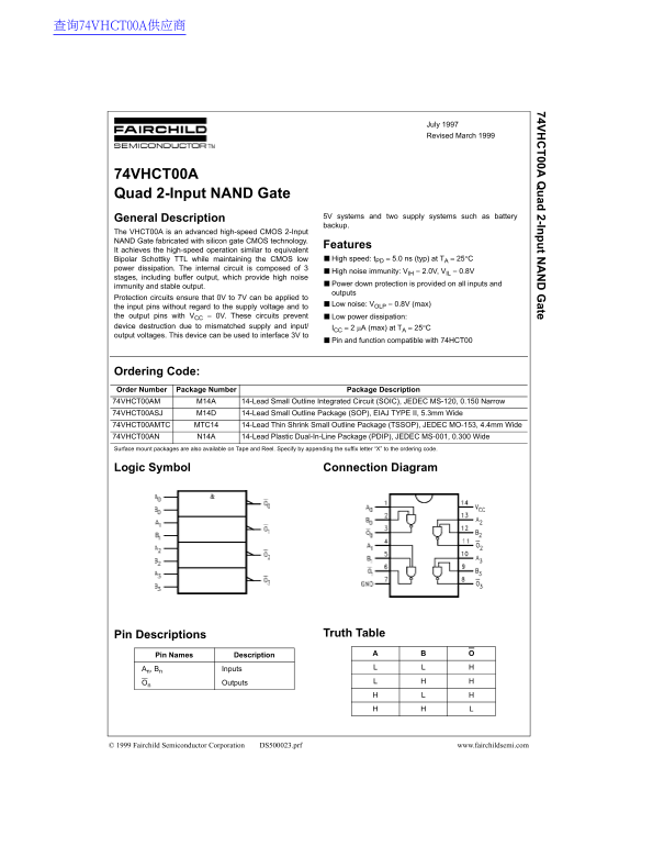
Page 1 Text Content
查询74VHCT00A供应商
74V 00A ad 2-In t N ate
July 1997 Revised March 1999
74VHCT00A Quad 2-Input NAND Gate
5V systems and two supply systems such as battery
General Description
backup.
The VHCT00A is an advanced high-speed CMOS 2-Input NAND Gate fabricated with silicon gate CMOS technology.
Features
It achieves the high-speed operation similar to equivalent
Bipolar Schottky TTL while maintaining the CMOS low High speed: t PD = 5.0 ns (typ) at TA = 25°C
power dissipation. The internal circuit is composed of 3
High noise immunity: VIH = 2.0V, VIL = 0.8V
stages, including buffer output, which provide high noise
Power down protection is provided on all inputs and
immunity and stable output.
outputs
Protection circuits ensure that 0V to 7V can be applied to
Low noise: VOLP = 0.8V (max)
the input pins without regard to the supply voltage and to the output pins with VCC = 0V. These circuits prevent Low power dissipation: device destruction due to mismatched supply and input/ ICC = 2 µA (max) at TA = 25°C output voltages. This device can be used to interface 3V to
Pin and function compatible with 74HCT00
Ordering Code: Order Number Package Number Package Description 74VHCT00AM M14A 14-Lead Small Outline Integrated Circuit (SOIC), JEDEC MS-120, 0.150 Narrow 74VHCT00ASJ M14D 14-Lead Small Outline Package (SOP), EIAJ TYPE II, 5.3mm Wide 74VHCT00AMTC MTC14 14-Lead Thin Shrink Small Outline Package (TSSOP), JEDEC MO-153, 4.4mm Wide 74VHCT00AN N14A 14-Lead Plastic Dual-In-Line Package (PDIP), JEDEC MS-001, 0.300 Wide Surface mount packages are also available on Tape and Reel. Specify by appending the suffix letter “X” to the ordering code.
Logic Symbol Connection Diagram
Pin Descriptions Truth Table
Pin Names Description
An, Bn Inputs
On Outputs
© 1999 Fairchild Semiconductor Corporation DS500023.prf www.fairchildsemi.com
Page Summary Contents For Fairchild 74VHCT00A Quad 2-Input NAND Gate Data Sheet
Manual Details
| Brand | Fairchild |
|---|---|
| Pages | 6 |
| File Size | 77.49 KB |
| Published | June 16, 2026 |
Enter the captcha to get the download link:

Frequently Asked Questions
What type of operation is supported by this device?
It supports high-speed operation similar to Bipolar Schottky TTL while maintaining CMOS benefits.
How does the device prevent damage from mismatched supply voltages?
It includes protection circuits that apply to input and output pins, preventing destruction due to mismatched supplies.
What is the typical maximum dynamic input voltage for this gate at 5.0V supply?
The V_ILD (Max Low Level Dynamic Input Voltage) is typically 0.8V with a capacitance of 50 pF.
Does this chip function with older series like the 74HCT00?
Yes, the device can be used to interface 3V and functions compatible with 74HCT00.