Fairchild MM74HC00 Quad 2-Input NAND Gate Data Sheet
Summary
This advanced Quad 2-Input NAND Gate utilizes robust CMOS technology for optimizing digital logic circuits. Ideal for hardware designers, engineers, and prototypers building low-power, high-reliability electronic systems that require dependable gating functions. The comprehensive manual details optimal operating conditions, electrical specifications, pin assignments, and multiple professional packaging options (DIP, SOIC, SOP), ensuring seamless integration into any design project.
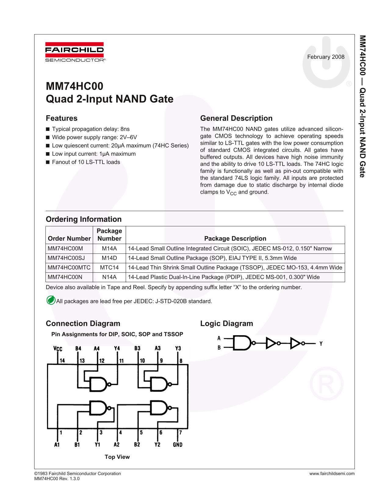
Page 1 Text Content
74H 00 — ad 2-In t N ate
February 2008
MM74HC00 Quad 2-Input NAND Gate Features General Description Typical propagation delay: 8ns The MM74HC00 NAND gates utilize advanced silicon-
Wide power supply range: 2V–6V gate CMOS technology to achieve operating speeds similar to LS-TTL gates with the low power consumption
Low quiescent current: 20µA maximum (74HC Series)
of standard CMOS integrated circuits. All gates have
Low input current: 1µA maximum
buffered outputs. All devices have high noise immunity
Fanout of 10 LS-TTL loads
and the ability to drive 10 LS-TTL loads. The 74HC logic family is functionally as well as pin-out compatible with the standard 74LS logic family. All inputs are protected from damage due to static discharge by internal diode clamps to VCC and ground.
Ordering Information
Package
Order Number Number Package Description MM74HC00M M14A 14-Lead Small Outline Integrated Circuit (SOIC), JEDEC MS-012, 0.150" Narrow MM74HC00SJ M14D 14-Lead Small Outline Package (SOP), EIAJ TYPE II, 5.3mm Wide MM74HC00MTC MTC14 14-Lead Thin Shrink Small Outline Package (TSSOP), JEDEC MO-153, 4.4mm Wide MM74HC00N N14A 14-Lead Plastic Dual-In-Line Package (PDIP), JEDEC MS-001, 0.300" Wide Device also available in Tape and Reel. Specify by appending suffix letter “X” to the ordering number.
All packages are lead free per JEDEC: J-STD-020B standard.
Connection Diagram Logic Diagram Pin Assignments for DIP, SOIC, SOP and TSSOP
Top View
©1 983 Fairchild Semiconductor Corporation www.fairchildsemi.com MM 74HC00 Rev. 1.3.0
Page Summary Contents For Fairchild MM74HC00 Quad 2-Input NAND Gate Data Sheet
Manual Details
| Brand | Fairchild |
|---|---|
| Pages | 9 |
| File Size | 317.41 KB |
| Published | July 07, 2026 |
Enter the captcha to get the download link:

Frequently Asked Questions
What is the recommended operating temperature range?
The device operates optimally in a temperature range of -40°C to +85°C.
What are the typical operational speeds and power requirements?
It has a typical propagation delay of 8ns, supports a wide supply range (2V–6V), and consumes low quiescent current (20µA max).
Does this logic family work with older circuits?
The 74HC family is functionally and pin-out compatible with the standard 74LS logic family.
Are there different packages available for ordering?
Yes, it is available in SOIC (MM74HC00M), SOP (MM74HC00SJ), TSSOP (MM74HC00MTC), and PDIP (MM74HC00N) packages.