STM M74HC00 Quad 2-Input NAND Gate Data Sheet Manual
Summary
Experience reliable digital logic with the M74HC00 Quad 2-Input NAND Gate, a high-speed CMOS component built for robust circuit protection and efficiency. This comprehensive manual is designed for electronics engineers and hardware designers, providing critical technical data for integration into embedded systems. It covers detailed electrical characteristics, absolute maximum ratings, timing parameters, low power dissipation specifications, and wide operating voltage ranges (2V to 6V), ensuring reliable performance in demanding real-world applications.
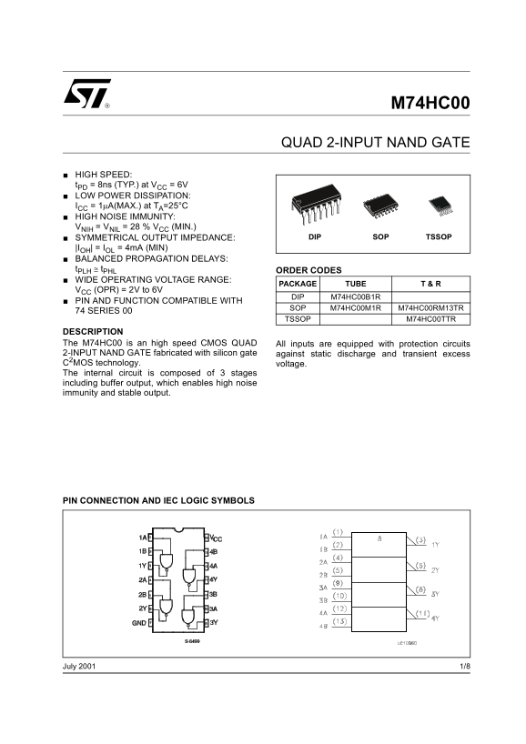
Page 1 Text Content
M74HC00
QUAD 2-INPUT NAND GATE
HIGH SPEED: t PD = 8ns (TYP.) at VCC = 6V LOW POWER DISSIPATION: ICC = 1µA(MAX.) at TA=25°C HIGH NOISE IMMUNITY: VNIH = VNIL = 28 % VCC (MIN.)
SYMMETRICAL OUTPUT IMPEDANCE: SOP TSSOPDIP
|IOH| = IOL = 4m A (MIN) BALANCED PROPAGATION DELAYS: t PLH ≅ t PHL ORDER CODES WIDE OPERATING VOLTAGE RANGE:
PACKAGE TUBE T & R
VCC (OPR) = 2V to 6V
DIP M74HC00B1R
PIN AND FUNCTION COMPATIBLE WITH
SOP M74HC00M1R M74HC00RM13TR
74 SERIES 00
TSSOP M74HC00TTR
DESCRIPTION The M74HC00 is an high speed CMOS QUAD All inputs are equipped with protection circuits 2-INPUT NAND GATE fabricated with silicon gate against static discharge and transient excess C2MOS technology. voltage. The internal circuit is composed of 3 stages including buffer output, which enables high noise immunity and stable output.
PIN CONNECTION AND IEC LOGIC SYMBOLS
1/8July 2001
Page Summary Contents For STM M74HC00 Quad 2-Input NAND Gate Data Sheet Manual
Manual Details
| Brand | QUAD |
|---|---|
| Pages | 8 |
| File Size | 178.61 KB |
| Published | May 27, 2026 |
Enter the captcha to get the download link:

Frequently Asked Questions
What is the recommended operating voltage range?
The recommended supply voltage (VCC) is between 2V and 6V.
Are the inputs protected from static discharge?
Yes, all inputs are equipped with protection circuits against static discharge and transient excess voltage.
How do I derate power dissipation for higher temperatures?
Power dissipation of 500mW is valid at 65°C; it must be derated to 300mW by 10mW/°C when operating between 65°C and 85°C.
What are the minimum required output current specifications?
The recommended low level output (OL) current is -4.0 mA at 4.5V and -5.2 mA at 6.0V.