Radiation Hardened Quad 2-Input OR Gate Data Sheet
Summary
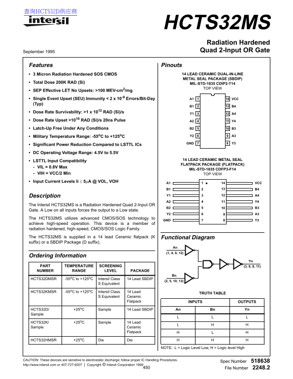
This Radiation Hardened Quad 2-Input OR Gate delivers high reliability using advanced CMOS/SOS technology. Ideal for mission-critical applications in aerospace and defense sectors that mandate performance under extreme conditions, including radiation exposure and wide temperature ranges (-55°C to +125°C). The comprehensive manual provides detailed electrical specifications, absolute maximum ratings, packaging details (SBDIP or Flatpack), and guidelines necessary for accurate system design and integration.
Page 1 Text Content
查询HCTS32D供应商
HCTS32MS Radiation Hardened September 1995 Quad 2-Input OR Gate
Features Pinouts
3 Micron Radiation Hardened SOS CMOS 14 LEAD CERAMIC DUAL-IN-LINE METAL SEAL PACKAGE (SBDIP)
Total Dose 200K RAD (Si)
MIL-STD-1835 CDIP2-T14 TOP VIEW
SEP Effective LET No Upsets: >100 MEV-cm2/mg Single Event Upset (SEU) Immunity < 2 x 10⁻⁹ Errors/Bit-Day A1 VCC (Typ)
Dose Rate Survivability: >1 x 10¹² RAD (Si)/s
Dose Rate Upset >1010 RAD (Si)/s 20ns Pulse A2 Y4
Latch-Up Free Under Any Conditions B2 B3
Military Temperature Range: -55o C to +125o C Y2 A3
GND Y3
Significant Power Reduction Compared to LSTTL ICs DC Operating Voltage Range: 4.5V to 5.5V
14 LEAD CERAMIC METAL SEAL
LSTTL Input Compatibility
FLATPACK PACKAGE (FLATPACK)
VIL = 0.8V Max
MIL-STD-1835 CDFP3-F14
VIH = VCC/2 Min TOP VIEW
Input Current Levels Ii ≤ 5µA @ VOL, VOH
1A1 VCC
B1 B4 Description Y1 A4 A2 Y4
The Intersil HCTS32MS is a Radiation Hardened Quad 2-Input OR
Gate. A Low on all inputs forces the output to a Low state.
The HCTS32MS utilizes advanced CMOS/SOS technology to
GND Y3
achieve high-speed operation. This device is a member of radiation hardened, high-speed, CMOS/SOS Logic Family. The HCTS32MS is supplied in a 14 lead Ceramic flatpack (K Functional Diagram suffix) or a SBDIP Package (D suffix).
An (1, 4, 9, 12)
Ordering Information
PART TEMPERATURE SCREENING (3, 6, 8, 11) NUMBER RANGE LEVEL PACKAGE
HCTS32DMSR -55o C to +125o C Intersil Class 14 Lead SBDIP
S Equivalent
HCTS32KMSR -55o C to +125o C Intersil Class 14 Lead
TRUTH TABLE
S Equivalent Ceramic
Flatpack INPUTS OUTPUTS
HCTS32D/ +25o C Sample 14 Lead SBDIP An Bn Yn Sample
HCTS32K/ +25o C Sample 14 Lead Sample Ceramic
Flatpack
HCTS32HMSR +25o C Die Die
NOTE: L = Logic Level Low, H = Logic level High
CAUTION: These devices are sensitive to electrostatic discharge; follow proper IC Handling Procedures.
Spec Number
http://www.intersil.com or 407-727-9207 Copyright © Intersil Corporation 1999
File Number 2248.2
Page Summary Contents For Radiation Hardened Quad 2-Input OR Gate Data Sheet
Manual Details
| Brand | QUAD |
|---|---|
| Pages | 9 |
| File Size | 57.67 KB |
| Published | May 27, 2026 |
Enter the captcha to get the download link:

Frequently Asked Questions
What is the recommended operating voltage range?
The device operates within a VCC range of 4.5V to 5.5V.
Are there specific warnings regarding handling this IC?
Yes, these devices are sensitive to electrostatic discharge (ESD); proper IC Handling Procedures must be followed.
In what package types is the HCTS32MS available?
It can be supplied in a Ceramic Flatpack (K suffix) or an SBDIP Package (D suffix).
What are the extreme temperature limitations?
The operational temperature range is -55°C to +125°C, with a storage range of -65°C to +150°C.