ST 74VHCT08A QUAD 2-INPUT AND GATE Data Sheet
Summary
The 74VHCT08A is a high-speed CMOS Quad 2-Input AND gate designed for digital logic interfaces. This advanced chip offers TTL compatibility and improved latch-up immunity while providing superior ESD protection circuits, ensuring reliable performance across varied voltage levels (e.g., 3V to 5V). The comprehensive datasheet covers detailed electrical characteristics, absolute maximum ratings, operating ranges, timing parameters, and pin functionality necessary for integrating this gate into complex digital systems. Ideal for electronics engineers and hardware designers requiring stable, low-noise, and high-speed AND gate circuitry.
Page 1 Text Content
74VHCT08A
QUAD 2-INPUT AND GATE
HIGH SPEED: t PD = 4.7 ns (TYP.) at VCC = 5V LOW POWER DISSIPATION: ICC = 2 µA (MAX.) at TA=25°C COMPATIBLE WITH TTL OUTPUTS: VIH = 2V (MIN.), VIL = 0.8V (MAX) POWER DOWN PROTECTION ON INPUTS
& OUTPUTS TSSOPSOP
SYMMETRICAL OUTPUT IMPEDANCE: |IOH| = IOL = 8 m A (MIN)
Table 1: Order Codes
BALANCED PROPAGATION DELAYS: t PLH ≅ t PHL
PACKAGE T & R
OPERATING VOLTAGE RANGE:
SOP 74VHCT08AMTR
VCC(OPR) = 4.5V to 5.5V
TSSOP 74VHCT08ATTR
PIN AND FUNCTION COMPATIBLE WITH 74 SERIES 08 IMPROVED LATCH-UP IMMUNITY Power down protection is provided on all inputs
LOW NOISE: VOLP = 0.8V (MAX.) and outputs and 0 to 7V can be accepted on inputs with no regard to the supply voltage. This DESCRIPTION device can be used to interface 5V to 3V since all inputs are equipped with TTL threshold.
The 74VHCT08A is an advanced high-speed
All inputs and outputs are equipped with
CMOS QUAD 2-INPUT AND GATE fabricated
protection circuits against static discharge, giving
with sub-micron silicon gate and double-layer
them 2KV ESD immunity and transient excess
metal wiring C2MOS technology.
voltage.
The internal circuit is composed of 2 stages including buffer output, which provides high noise immunity and stable output.
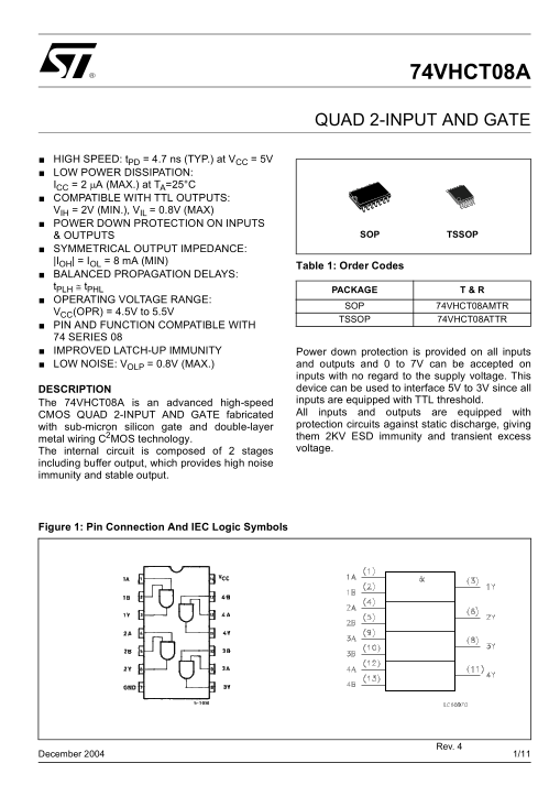
Figure 1: Pin Connection And IEC Logic Symbols
Rev. 4
1/11December 2004
Page Summary Contents For ST 74VHCT08A QUAD 2-INPUT AND GATE Data Sheet
Manual Details
| Brand | QUAD |
|---|---|
| Pages | 11 |
| File Size | 206.50 KB |
| Published | May 29, 2026 |
Enter the captcha to get the download link:

Frequently Asked Questions
Is this device compatible with TTL level signals?
Yes, the inputs are equipped with TTL threshold, allowing it to interface between 5V and 3V. It is also listed as compatible with TTL outputs.
What protection features are included against electrical spikes?
The IC includes fabricated protection circuits against static discharge (ESD), offering 2KV immunity.
What is the recommended operating voltage range for VCC?
The specified operating voltage range (VCC) is 4.5 to 5.5V, with a typical quiescent supply current of 220 μA.
What are its environmental operating limits?
It can operate across an ambient temperature range of -55°C to 125°C.