Fairchild 74LVX00 Low-Voltage Quad 2-Input NAND Gate Data Manual
Summary
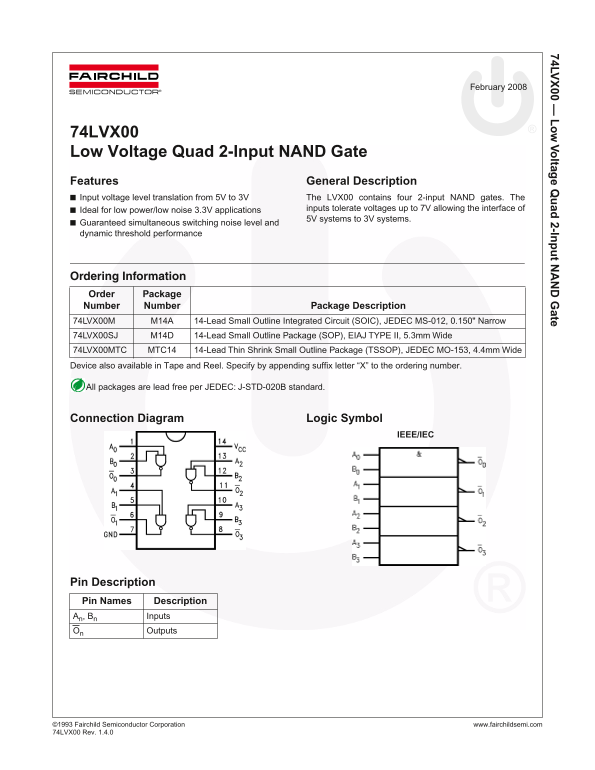
This manual details the 74LVX00, a low voltage quad 2-input NAND gate designed for 3.3V applications. It covers electrical characteristics, operating conditions, and pin configurations, making it ideal for engineers and technicians working on low-power digital interface systems.
Page 1 Text Content
74LV 00 — Vo ltag e Q ad 2-In t N ate
February 2008
74LVX00 Low Voltage Quad 2-Input NAND Gate Features General Description Input voltage level translation from 5V to 3V The LVX00 contains four 2-input NAND gates. The
Ideal for low power/low noise 3.3V applications inputs tolerate voltages up to 7V allowing the interface of 5V systems to 3V systems.
Guaranteed simultaneous switching noise level and dynamic threshold performance
Ordering Information Order Package Number Number Package Description 74LVX00M M14A 14-Lead Small Outline Integrated Circuit (SOIC), JEDEC MS-012, 0.150" Narrow 74LVX00SJ M14D 14-Lead Small Outline Package (SOP), EIAJ TYPE II, 5.3mm Wide 74LVX00MTC MTC14 14-Lead Thin Shrink Small Outline Package (TSSOP), JEDEC MO-153, 4.4mm Wide Device also available in Tape and Reel. Specify by appending suffix letter “X” to the ordering number.
All packages are lead free per JEDEC: J-STD-020B standard.
Connection Diagram Logic Symbol
IEEE/IEC
Pin Description Pin Names Description An, Bn Inputs
On Outputs
©1 993 Fairchild Semiconductor Corporation www.fairchildsemi.com 74L VX00 Rev. 1.4.0
Page Summary Contents For Fairchild 74LVX00 Low-Voltage Quad 2-Input NAND Gate Data Manual
Manual Details
| Brand | Fairchild |
|---|---|
| Pages | 8 |
| File Size | 300.59 KB |
| Published | June 15, 2026 |
Enter the captcha to get the download link:

Frequently Asked Questions
What is the supply voltage range for the 74LVX00?
The recommended supply voltage range is 2.0V to 3.6V.
Can the 74LVX00 interface 5V systems to 3V systems?
Yes, inputs tolerate voltages up to 7V, allowing 5V systems to interface with 3V systems.
What is the maximum storage temperature?
The storage temperature range is -65°C to +150°C.
How should unused inputs be handled?
Unused inputs must be held HIGH or LOW and may not float.
What package options are available?
The device is available in SOIC, SOP, and TSSOP packages.