Fairchild 74LVX132 Low Voltage Quad 2-Input NAND Schmitt Trigger Data Manual
Summary
Fairchild Semiconductor 74LVX132 low voltage quad 2-input NAND Schmitt trigger datasheet. The document describes input voltage level translation from 5V to 3V, hysteresis characteristics for noise immunity, pin configurations, and electrical specifications for low-power 3.3V applications. Target users are digital design engineers implementing level-shifting and noise-resistant logic in mixed-voltage systems.
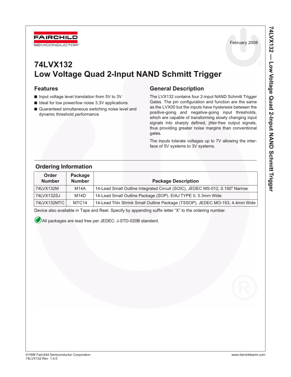
Page 1 Text Content
74LV 132 — Vo ltag e Q ad 2-In t N ch itt Trig er
February 2008
74LVX132 Low Voltage Quad 2-Input NAND Schmitt Trigger Features General Description Input voltage level translation from 5V to 3V The LVX132 contains four 2-input NAND Schmitt Trigger
Ideal for low power/low noise 3.3V applications Gates. The pin configuration and function are the same as the LVX00 but the inputs have hysteresis between the
Guaranteed simultaneous switching noise level and
positive-going and negative-going input thresholds,
dynamic threshold performance
which are capable of transforming slowly changing input signals into sharply defined, jitter-free output signals, thus providing greater noise margins than conventional gates. The inputs tolerate voltages up to 7V allowing the inter- face of 5V systems to 3V systems.
Ordering Information Order Package Number Number Package Description 74LVX132M M14A 14-Lead Small Outline Integrated Circuit (SOIC), JEDEC MS-012, 0.150" Narrow 74LVX132SJ M14D 14-Lead Small Outline Package (SOP), EIAJ TYPE II, 5.3mm Wide 74LVX132MTC MTC14 14-Lead Thin Shrink Small Outline Package (TSSOP), JEDEC MO-153, 4.4mm Wide Device also available in Tape and Reel. Specify by appending suffix letter “X” to the ordering number.
All packages are lead free per JEDEC: J-STD-020B standard.
©1 996 Fairchild Semiconductor Corporation www.fairchildsemi.com 74L VX132 Rev. 1.4.0
Page Summary Contents For Fairchild 74LVX132 Low Voltage Quad 2-Input NAND Schmitt Trigger Data Manual
Manual Details
| Brand | Fairchild |
|---|---|
| Pages | 9 |
| File Size | 332.60 KB |
| Published | June 17, 2026 |
Enter the captcha to get the download link:

Frequently Asked Questions
What is the main function of the 74LVX132?
It translates input voltage levels from 5V to 3V and provides four NAND Schmitt trigger gates for noise immunity.
What is the recommended operating voltage range?
The supply voltage (V_CC) should be between 2.0V and 3.6V.
Can unused inputs be left disconnected?
No, unused inputs must be held HIGH or LOW and cannot be left floating.
What packages is the 74LVX132 available in?
It is available in SOIC, SOP, and TSSOP 14-lead packages, all lead-free.
What is the maximum input voltage tolerance?
Inputs can tolerate voltages up to 7V, allowing interface between 5V and 3V systems.