Fairchild 74VHC132 Quad 2-Input NAND Schmitt Trigger Data Manual
Summary
The 74VHC132 is an advanced high-speed CMOS Quad 2-Input NAND Schmitt Trigger gate. This high-speed, low-power device transforms slowly changing input signals into jitter-free outputs, offering excellent noise immunity and pin compatibility with the 74HC132. Designed for use in 5V to 3V systems, it features input protection and is available in lead-free SOIC, SOP, and TSSOP packages.
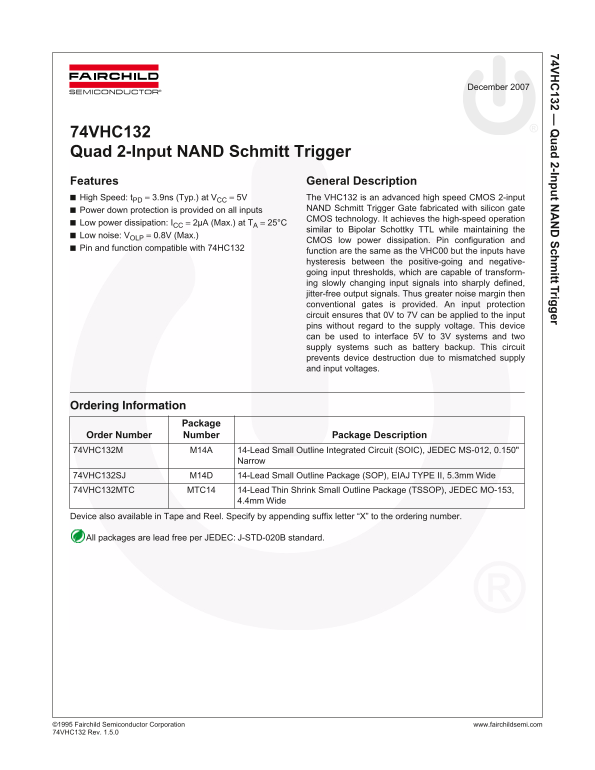
Page 1 Text Content
74V 132 — ad 2-In t N ch itt Trig er
December 2007
74VHC132 Quad 2-Input NAND Schmitt Trigger Features General Description High Speed: t PD = 3.9ns (Typ.) at VCC = 5V The VHC132 is an advanced high speed CMOS 2-input
Power down protection is provided on all inputs NAND Schmitt Trigger Gate fabricated with silicon gate CMOS technology. It achieves the high-speed operation
Low power dissipation: ICC = 2µA (Max.) at TA = 25°C
similar to Bipolar Schottky TTL while maintaining the
Low noise: VOLP = 0.8V (Max.)
CMOS low power dissipation. Pin configuration and
Pin and function compatible with 74HC132
function are the same as the VHC00 but the inputs have hysteresis between the positive-going and negative- going input thresholds, which are capable of transform- ing slowly changing input signals into sharply defined, jitter-free output signals. Thus greater noise margin then conventional gates is provided. An input protection circuit ensures that 0V to 7V can be applied to the input pins without regard to the supply voltage. This device can be used to interface 5V to 3V systems and two supply systems such as battery backup. This circuit prevents device destruction due to mismatched supply and input voltages.
Ordering Information
Package
Order Number Number Package Description 74VHC132M M14A 14-Lead Small Outline Integrated Circuit (SOIC), JEDEC MS-012, 0.150"
Narrow
74VHC132SJ M14D 14-Lead Small Outline Package (SOP), EIAJ TYPE II, 5.3mm Wide 74VHC132MTC MTC14 14-Lead Thin Shrink Small Outline Package (TSSOP), JEDEC MO-153,
4.4mm Wide
Device also available in Tape and Reel. Specify by appending suffix letter “X” to the ordering number.
All packages are lead free per JEDEC: J-STD-020B standard.
©1 995 Fairchild Semiconductor Corporation www.fairchildsemi.com 74V HC132 Rev. 1.5.0
Page Summary Contents For Fairchild 74VHC132 Quad 2-Input NAND Schmitt Trigger Data Manual
Manual Details
| Brand | Fairchild |
|---|---|
| Pages | 9 |
| File Size | 317.54 KB |
| Published | June 15, 2026 |
Enter the captcha to get the download link:

Frequently Asked Questions
What is the purpose of the hysteresis in the 74VHC132?
It transforms slowly changing input signals into sharply defined, jitter-free output signals and provides greater noise margin than conventional gates.
Can the 74VHC132 be used for 5V to 3V system interfacing?
Yes, it can interface 5V to 3V systems and two-supply systems such as battery backup, because inputs tolerate 0V to 7V regardless of supply voltage.
What is the recommended operating supply voltage range for the 74VHC132?
The recommended supply voltage (VCC) is 2.0V to +5.5V.
How does the 74VHC132 protect against mismatched supply and input voltages?
An input protection circuit allows 0V to 7V on input pins without regard to supply voltage, preventing device destruction from mismatched supplies.
Is the 74VHC132 pin and function compatible with the 74HC132?
Yes, it is pin and function compatible with the 74HC132.