ST M74HC7266 Quad Exclusive NOR Gate Data Sheet
Summary
A robust M74HC7266 is a high-speed CMOS Quad Exclusive NOR Gate IC, engineered for reliable digital logic with exceptional noise immunity and low power consumption. This manual details comprehensive technical data, including full electrical specifications, absolute maximum ratings, performance graphs, and operating conditions across various package types. It serves electronics engineers and circuit designers who require stable, high-performance gates for complex and demanding digital systems.
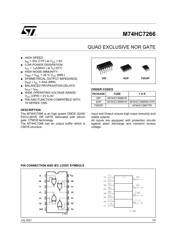
Page 1 Text Content
M74HC7266
QUAD EXCLUSIVE NOR GATE
HIGH SPEED: t PD = 9ns (TYP.) at VCC = 6V LOW POWER DISSIPATION: ICC = 1µA(MAX.) at TA=25°C HIGH NOISE IMMUNITY: VNIH = VNIL = 28 % VCC (MIN.)
SYMMETRICAL OUTPUT IMPEDANCE: SOP TSSOPDIP
|IOH| = IOL = 4m A (MIN) BALANCED PROPAGATION DELAYS: t PLH ≅ t PHL ORDER CODES WIDE OPERATING VOLTAGE RANGE:
PACKAGE TUBE T & R
VCC (OPR) = 2V to 6V
DIP M74HC7266B1R
PIN AND FUNCTION COMPATIBLE WITH
SOP M74HC7266M1R M74HC7266RM13TR
74 SERIES 7266
TSSOP M74HC7266TTR
DESCRIPTION The M74HC7266 is an high speed CMOS QUAD Input and Output ensure high noise immunity and EXCLUSIVE OR GATE fabricated with silicon stable outputs. gate C2MOS technology All inputs are equipped with protection circuits The M74HC7266 has an output buffer which is against static discharge and transient excess CMOS structure. voltage.
PIN CONNECTION AND IEC LOGIC SYMBOLS
1/9July 2001
Page Summary Contents For ST M74HC7266 Quad Exclusive NOR Gate Data Sheet
Manual Details
| Brand | QUAD |
|---|---|
| Pages | 9 |
| File Size | 170.39 KB |
| Published | May 29, 2026 |
Enter the captcha to get the download link:

Frequently Asked Questions
What is the recommended operating voltage range for this device?
The recommended supply voltage (VCC) operates between 2V and 6V.
How are propagation delays affected by different voltages?
At 4.5V, the minimum propagation delay is 90ns (PLH) and 115ns (PHL). At 6.0V, they are 152ns (PLH) and 202ns (PHL).
Does this chip have internal protection features?
Yes, all inputs are equipped with protection circuits, and the output buffer is protected against static discharge and transient excess voltage.
What is the specified operating temperature range?
The recommended operating temperature range is -55°C to 125°C.