Toshiba TOSHIBA Multi-Chip Transistor Silicon NPN Epitaxial Type, Field Effect Transistor Silicon N Channel MOS Type TPCP8H01 Data Sheet
Summary
The TPCP8H01 is a high-speed, multi-chip discrete transistor expertly combining NPN logic with an N-channel MOS FET structure. Ideal for demanding applications like strobe flash and general signal switching, this component offers reliable performance through its integrated architecture. This comprehensive manual provides detailed electrical characteristics, absolute ratings, and essential design curves (including turn/off times) necessary for engineers requiring precision IC integration in industrial, computing, or measurement equipment.
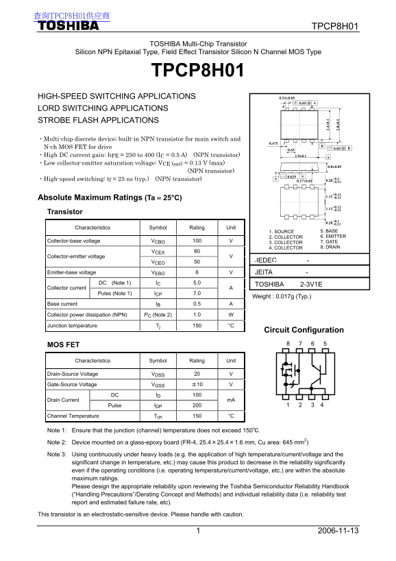
Page 1 Text Content
查询TPCP8H01供应商
TPCP8H01
TOSHIBA Multi-Chip Transistor Silicon NPN Epitaxial Type, Field Effect Transistor Silicon N Channel MOS Type
TPCP8H01
HIGH-SPEED SWITCHING APPLICATIONS 0.33±0.05
LORD SWITCHING APPLICATIONS STROBE FLASH APPLICATIONS
・Multi-chip discrete device; built-in NPN transistor for main switch and
N-ch MOS FET for drive B0.05
・High DC current gain: h FE = 250 to 400 (IC = 0.5 A) (NPN transistor) 2.9±0.1 ・Low collector-emitter saturation voltage: VCE (sat) = 0.13 V (max)
(NPN transistor)
・High-speed switching: tf = 25 ns (typ.) (NPN transistor) 0.17±0.02 0.28+0.1
Absolute Maximum Ratings (Ta = 25°C)
Transistor
Characteristics Symbol Rating Unit
1. SOURCE 5. BASE 2. COLLECTOR 6. EMITTER
Collector-base voltage VCBO 100 V 7. GATE
3. COLLECTOR
4. COLLECTOR 8. DRAIN
VCEX 80
Collector-emitter voltage
VCEO 50 JEDEC
Emitter-base voltage VEBO 6 V JEITA
DC (Note 1) IC 5.0
TOSHIBA 2-3V1E
Collector current
Pulse (Note 1) ICP 7.0
Weight : 0.017g (Typ.)
Base current IB 0.5 A
Collector power dissipation (NPN) PC (Note 2) 1.0 W
Junction temperature Tj 150 °C
Circuit Configuration
MOS FET
Characteristics Symbol Rating Unit
Drain-Source Voltage VDSS 20 V
Gate-Source Voltage VGSS ±10 V
DC ID 100
Drain Current m A
Pulse IDP 200 1 2 3 4
Channel Temperature Tch 150 °C
Note 1: Ensure that the junction (channel) temperature does not exceed 150℃.
Note 2: Device mounted on a glass-epoxy board (FR-4, 25.4×25.4×1.6 mm, Cu area: 645 mm2) Note 3: Using continuously under heavy loads (e.g. the application of high temperature/current/voltage and the
significant change in temperature, etc.) may cause this product to decrease in the reliability significantly even if the operating conditions (i.e. operating temperature/current/voltage, etc.) are within the absolute maximum ratings. Please design the appropriate reliability upon reviewing the Toshiba Semiconductor Reliability Handbook (“Handling Precautions”/Derating Concept and Methods) and individual reliability data (i.e. reliability test report and estimated failure rate, etc).
This transistor is an electrostatic-sensitive device. Please handle with caution.
Page Summary Contents For Toshiba TOSHIBA Multi-Chip Transistor Silicon NPN Epitaxial Type, Field Effect Transistor Silicon N Channel MOS Type TPCP8H01 Data Sheet
Manual Details
| Brand | Toshiba |
|---|---|
| Pages | 8 |
| File Size | 246.76 KB |
| Published | May 29, 2026 |
Enter the captcha to get the download link:

Frequently Asked Questions
What types of applications are strictly prohibited for this product?
It is not meant for use in life-critical systems such as airplane instruments, medical devices, or transportation control equipment.
How must I design the circuit board for maximum reliability?
The device should be mounted on a glass-epoxy board (FR-4), and you must review the Toshiba Reliability Handbook to implement proper derating.
What critical warning exists regarding high usage or temperature changes?
Continuous use under heavy load, especially with significant temperature changes, can severely reduce reliability even if initial ratings are met.