Toshiba Field-Effect Transistor Silicon P-Channel MOS Type SSM3J117TU Data Manual
Summary
This comprehensive manual details the SSM3J117TU, a high-performance Silicon P-Channel MOSFET (Field-Effect Transistor). It provides essential technical specifications, including detailed electrical characteristics for switching time, low ON-resistance ($R_{DS(ON)}$), and output capacitance. This resource is vital for electronics engineers and designers requiring reliable components for general high-speed switching applications in consumer, industrial, or computing equipment. The guide also covers absolute maximum ratings and handling precautions to ensure proper device integration and longevity.
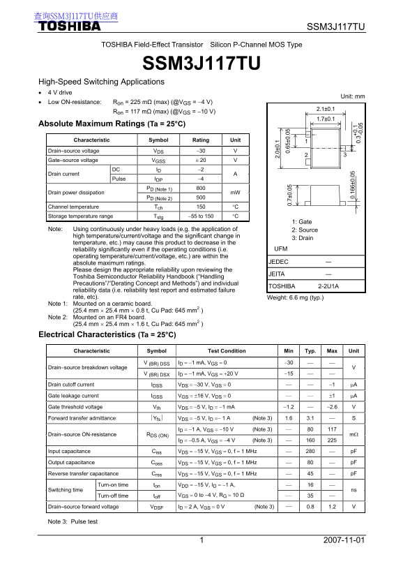
Page 1 Text Content
查询SSM3J117TU供应商
SSM3J117TU
TOSHIBA Field-Effect Transistor Silicon P-Channel MOS Type
SSM3J117TU
High-Speed Switching Applications • 4 V drive
Unit: mm
• Low ON-resistance: Ron = 225 mΩ (max) (@VGS = −4 V)
Ron = 117 mΩ (max) (@VGS = −10 V)
Absolute Maximum Ratings (Ta = 25°C)
Characteristic Symbol Rating Unit
Drain–source voltage VDS −30 V
Gate–source voltage VGSS ± 20 V
DC ID −2
Drain current
Pulse IDP −4
PD (Note 1) 800
Drain power dissipation m W
PD (Note 2) 500
Channel temperature Tch 150 °C Storage temperature range Tstg −55 to 150 °C
1: Gate
Note: Using continuously under heavy loads (e.g. the application of 2: Source
high temperature/current/voltage and the significant change in
3: Drain
temperature, etc.) may cause this product to decrease in the
reliability significantly even if the operating conditions (i.e. UFM
operating temperature/current/voltage, etc.) are within the
absolute maximum ratings. JEDEC ―
Please design the appropriate reliability upon reviewing the
JEITA ―
Toshiba Semiconductor Reliability Handbook (“Handling 0± 0. Precautions”/“Derating Concept and Methods”) and individual
TOSHIBA 2-2U1A
reliability data (i.e. reliability test report and estimated failure 0. 7± 0.
rate, etc). Weight: 6.6 mg (typ.)
Note 1: Mounted on a ceramic board.
(25.4 mm × 25.4 mm × 0.8 t, Cu Pad: 645 mm2 )
Note 2: Mounted on an FR4 board.
(25.4 mm × 25.4 mm × 1.6 t, Cu Pad: 645 mm2 )
Electrical Characteristics (Ta = 25°C)
Characteristic Symbol Test Condition Min Typ. Max Unit
V (BR) DSS ID = −1 m A, VGS = 0 −30 ⎯ ⎯
Drain–source breakdown voltage
V (BR) DSX ID = −1 m A, VGS = +20 V −15 ⎯ ⎯
Drain cutoff current IDSS VDS = −30 V, VGS = 0 ⎯ ⎯ −1 μA
Gate leakage current IGSS VGS = ±16 V, VDS = 0 ⎯ ⎯ ±1 μA
Gate threshold voltage Vth VDS = −5 V, ID = −1 m A −1.2 ⎯ −2.6
Forward transfer admittance ⏐Yfs⏐ VDS = −5 V, ID =− 1 A (Note 3) 1.6 3.1 ⎯ S
ID = −1 A, VGS = −10 V (Note 3) ⎯ 80 117
Drain–source ON-resistance RDS (ON) mΩ
ID = −0.5 A, VGS = −4 V (Note 3) ⎯ 160 225
Input capacitance Ciss VDS = −15 V, VGS = 0, f = 1 MHz ⎯ 280 ⎯ p F
Output capacitance Coss VDS = −15 V, VGS = 0, f = 1 MHz ⎯ 80 ⎯ p F
Reverse transfer capacitance Crss VDS = −15 V, VGS = 0, f = 1 MHz ⎯ 45 ⎯ p F
Turn-on time ton ⎯ 16 ⎯ VDD = −15 V, ID = −1 A,
Switching time ns
Turn-off time toff VGS = 0 to −4 V, RG = 10 Ω ⎯ 35 ⎯
Drain–source forward voltage VDSF ID = 2 A, VGS = 0 V (Note 3) ⎯ 0.8 1.2 V
Note 3: Pulse test
Page Summary Contents For Toshiba Field-Effect Transistor Silicon P-Channel MOS Type SSM3J117TU Data Manual
Manual Details
| Brand | Toshiba |
|---|---|
| Pages | 5 |
| File Size | 125.37 KB |
| Published | May 31, 2026 |
Enter the captcha to get the download link:

Frequently Asked Questions
What is the typical drain-source ON-resistance (Rds(on))?
At I = −1 A and V = −4 V, the low Rds(on) is typically 225 mΩ.
How does the gate threshold voltage relate to normal operating conditions?
For normal switching operation, the required Gate-Source voltage is generally higher than Vgh(on) and lower than Vgh(off).