Toshiba TOSHIBA CMOS Digital Integrated Circuit Silicon Monolithic TC7WG125FU,TC7WG125FK Data Manual
Summary
Enhance your digital design with this high-performance CMOS Dual Bus Buffer IC, featuring a 3-state output. This robust integrated circuit guarantees reliable signal transmission across various industrial applications, boasting high-speed operation and broad voltage tolerance up to 5.5V. The manual provides comprehensive technical documentation, detailing all electrical characteristics, AC specifications, and operational guidelines necessary for optimal integration into general electronics equipment like computing or automation systems.
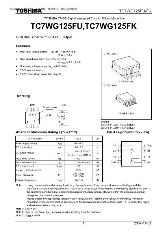
Page 1 Text Content
TC7WG125FU/FK
TOSHIBA CMOS Digital Integrated Circuit Silicon Monolithic
TC7WG125FU,TC7WG125FK Dual Bus Buffer with 3-STATE Output Features • High-level output current: IOH/IOL = ±8 m A (min)
TC7WG125FU
at VCC = 3 V • High-speed operation: tpd = 2.5 ns (typ.) at VCC = 3.3 V,15p F • Operating voltage range: VCC = 0.9~3.6 V • 5.5-V tolerant inputs • 3.6-V power down protection outputs
TC7WG125FK
Marking
SM8 US8
Product name
G 125 Lot. No WG
Weight SSOP8-P-0.65 : 0.02 g (typ.) SSOP8-P-0.50A : 0.01 g (typ.)
Absolute Maximum Ratings (Ta = 25°C) Pin Assignment (top view) Characteristics Symbol Value Unit Power supply voltage VCC −0.5~4.6 V
G1 VCC
DC input voltage VIN −0.5~7.0 V
−0.5~4.6 (Note 1) A1 G2
DC output voltage VOUT
−0.5~VCC + 0.5 (Note 2)
Input diode current IIK −20 m A
Output diode current IOK −20 (Note 3) m A GND A2
DC output current IOUT ±25 m A DC VCC / ground current ICC ±100 m A
Power dissipation PD 300 (SM8)
200 (US8) m W
Storage temperature Tstg −65~150 °C
Note: Using continuously under heavy loads (e.g. the application of high temperature/current/voltage and the
significant change in temperature, etc.) may cause this product to decrease in the reliability significantly even if the operating conditions (i.e. operating temperature/current/voltage, etc.) are within the absolute maximum ratings and the operating ranges. Please design the appropriate reliability upon reviewing the Toshiba Semiconductor Reliability Handbook (“Handling Precautions”/Derating Concept and Methods) and individual reliability data (i.e. reliability test report and estimated failure rate, etc).
Note 1: VCC = 0V Note 2: High or Low State. IOUT absolute maximum rating must be observed. Note 3: VOUT < GND
Page Summary Contents For Toshiba TOSHIBA CMOS Digital Integrated Circuit Silicon Monolithic TC7WG125FU,TC7WG125FK Data Manual
Manual Details
| Brand | Toshiba |
|---|---|
| Pages | 9 |
| File Size | 225.48 KB |
| Published | May 29, 2026 |
Enter the captcha to get the download link:

Frequently Asked Questions
What is the operating voltage range for this integrated circuit?
The operating voltage (Vcc) ranges from 0.9 V to 3.6 V.
Is there a limit on ambient temperature operation?
The product operates across an environmental temperature range of -40°C to 85°C.
What is the maximum output current rating?
The absolute maximum DC output current (I_OUT) is specified as ±25 mA.