Toshiba TOSHIBA BiCMOS Linear Integrated Circuit Silicon Monolithic TB6066FNG Owner's Manual
Summary
The TB6066FNG is a specialized Shock Sensor IC engineered for detecting external shock events across diverse systems. Featuring multiple built-in operational amplifiers and excellent Signal-to-Noise ratio, it supports precise analog detection suitable for advanced mechanical control applications, such as servo systems. This technical guide provides comprehensive details on specifications, pin functions, electrical performance ratings, and voltage requirements (2.7 to 5.5 V DC). It is essential documentation for electronics designers and engineers integrating reliable shock monitoring into industrial, measuring, or consumer equipment.
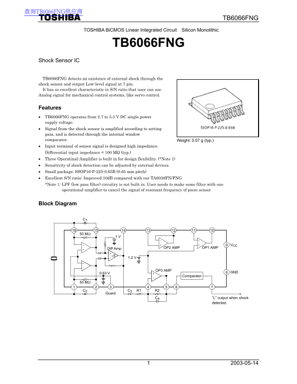
Page 1 Text Content
查询TB6066FNG供应商
TB6066FNG
TOSHIBA Bi CMOS Linear Integrated Circuit Silicon Monolithic
TB6066FNG
Shock Sensor IC
TB6066FNG detects an existence of external shock through the shock sensor and output Low-level signal at 7 pin. It has so excellent characteristic in S/N ratio that user can use Analog signal for mechanical control systems, like servo control.
Features • TB6066FNG operates from 2.7 to 5.5 V DC single power supply voltage. • Signal from the shock sensor is amplified according to setting gain, and is detected through the internal window comparator. Weight: 0.07 g (typ.) • Input terminal of sensor signal is designed high impedance. Differential input impedance = 100 MΩ (typ.) • Three Operatinal-Amplifier is built in for design flexibility. (*Note 1) • Sensitivity of shock detection can be adjusted by external devices. • Small package: SSOP16-P-225-0.65B (0.65 mm pitch) • Excellent S/N ratio: Improved 10d B compared with our TA6038FN/FNG *Note 1: LPF (low pass filter) circuitry is not bulit in. User needs to make some filter with one
operational-amplifier to cancel the signal of resonant frequency of piezo sensor
Block Diagram
9 VCC
Diff Amp OP2 AMP OP1 AMP
OP3 AMP
0.63 V 8 GND
Comparator
Guard
C4 “L” output when shock
detected.
Page Summary Contents For Toshiba TOSHIBA BiCMOS Linear Integrated Circuit Silicon Monolithic TB6066FNG Owner's Manual
Manual Details
| Brand | Toshiba |
|---|---|
| Pages | 14 |
| File Size | 240.00 KB |
| Published | June 01, 2026 |
Enter the captcha to get the download link:

Frequently Asked Questions
What is the recommended operating voltage range?
The device operates from 2.7 to 5.5 V DC single power supply voltage.
How should I filter the signal in my design?
Since LPF circuitry is not built-in, you must use an external operational amplifier to create a low pass filter and cancel resonant frequency signals.
What does the output pin indicate when a shock occurs?
Pin 7 (CMO) provides the output; it outputs a Low-level signal ("L") when a shock is detected.
What is the differential input impedance of the sensor?
The input terminal is designed with a high impedance, specifically a differential input impedance of 100 MΩ (typ.).