Toshiba TOSHIBA CMOS Digital Integrated Circuit Silicon Monolithic TC7SH126FE Data Sheet
Summary
The TC7SH126FE is a high-speed, low-power CMOS Bus Buffer integrated circuit designed for reliable signal level shifting. Featuring robust performance characteristics, including wide operating voltage ranges (2–5.5V) and high noise immunity, this component enhances system integrity in complex electronic designs. The accompanying manual provides comprehensive technical documentation, covering detailed DC/AC electrical specifications, timing diagrams, truth tables, and optimal operating conditions. This essential guide is intended for electronic engineers and circuit designers who require dependable components for general industrial, computing, or commercial equipment applications.
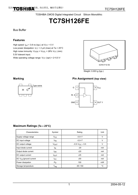
Page 1 Text Content
TC7SH126FE
TOSHIBA CMOS Digital Integrated Circuit Silicon Monolithic
TC7SH126FE
Bus Buffer
Features High speed: tpd = 3.8 ns (typ.) at VCC = 5 V Low power dissipation: ICC = 2 µA (max) at Ta = 25°C High noise immunity: VNIH = VNIL = 28% VCC (min) 5.5V tolerant input. Wide operating voltage range: VCC (opr) = 2~5.5 V
Weight: 0.003 g (typ.)
Marking Pin Assignment (top view)
Type name
H C IN A
GND OUT Y 3
Maximum Ratings (Ta = 25°C)
Characteristics Symbol Rating Unit
Supply voltage range VCC −0.5~7 V
DC input voltage VIN −0.5~7 V
DC output voltage VOUT −0.5~VCC + 0.5 V
Input diode current IIK −20 m A
Output diode current IOK ±20 m A
DC output current IOUT ±25 m A
DC VCC/ground current ICC ±50 m A
Power dissipation PD 150 m W
Storage temperature Tstg −65~150 °C
Page Summary Contents For Toshiba TOSHIBA CMOS Digital Integrated Circuit Silicon Monolithic TC7SH126FE Data Sheet
Manual Details
| Brand | Toshiba |
|---|---|
| Pages | 5 |
| File Size | 112.02 KB |
| Published | June 02, 2026 |
Enter the captcha to get the download link:

Frequently Asked Questions
What is the recommended operational voltage range for V_CC?
The recommended operating conditions specify a supply voltage (V) of 2 to 5.5 V.
How fast can this integrated circuit operate at standard voltages?
It features high speed, with a typical fall time (t) of 3.8 ns when operated at 5 V.
Can I use this chip in safety-critical systems like aircraft instruments?
No; the products are not warranted for 'Unintended Usage,' including equipment where failure could cause loss of life, such as medical or aerospace instruments.
Does this device offer a three-state output feature?
Yes, the AC characteristics provide dedicated parameters (t_pZH and t_pLZ) for 3-state output functionality.