# A B C D E F G H I J K L M N O P Q R S T U V W X Y Z

Toshiba TOSHIBA Bi-CMOS Integrated Circuit Silicon Monolithic TB6551F Data Sheet

Summary

This comprehensive guide details the Toshiba TB6551F semiconductor integrated circuit, a specialized 3-Phase Full-Wave Sine-Wave PWM Brushless Motor Controller. The manual covers detailed pin descriptions, electrical characteristic tables, and application circuits necessary for system integration. It provides precise control mechanisms, including adjustable lead angle setting (0°–58°), dead time function, and overcurrent protection. This product is essential for electronics engineers designing high-performance applications requiring accurate motor speed and direction control in various industrial and sophisticated consumer devices.
📄 Preview PAGE OF 18

Page 1 Text Content

查询TB6551F供应商

TB6551F

TOSHIBA Bi-CMOS Integrated Circuit Silicon Monolithic

TB6551F

3-Phase Full-Wave Sine-Wave PWM Brushless Motor Controller

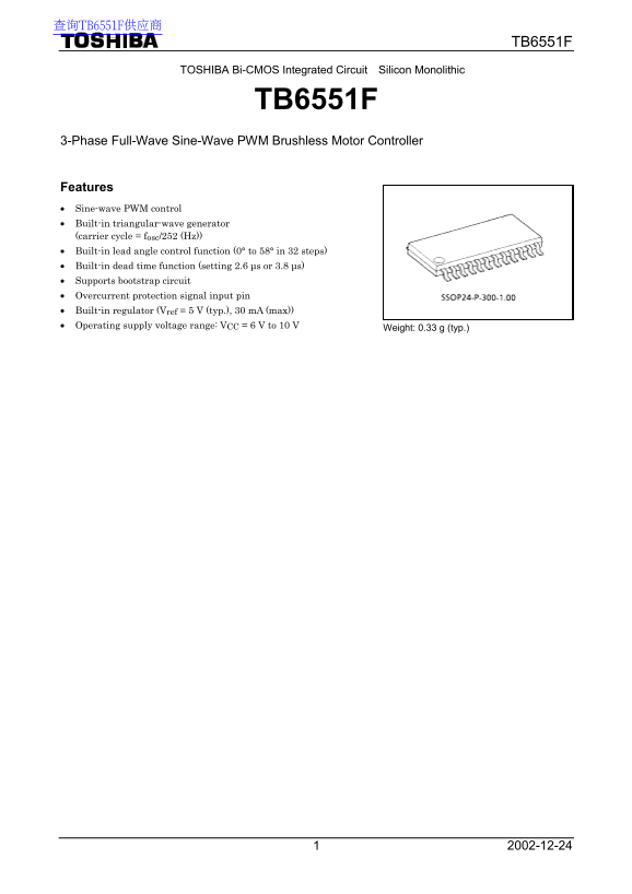
Features Sine-wave PWM control Built-in triangular-wave generator (carrier cycle = fosc/252 (Hz)) Built-in lead angle control function (0° to 58° in 32 steps) Built-in dead time function (setting 2.6 µs or 3.8 µs) Supports bootstrap circuit Overcurrent protection signal input pin Built-in regulator (Vref = 5 V (typ.), 30 m A (max)) Operating supply voltage range: VCC = 6 V to 10 V

Weight: 0.33 g (typ.)

Page Summary Contents For Toshiba TOSHIBA Bi-CMOS Integrated Circuit Silicon Monolithic TB6551F Data Sheet

Page 1 查询TB6551F供应商 TB6551F TOSHIBA Bi-CMOS Integrated Circuit Silicon Monolithic TB6551F 3-Phase Full-Wave Sine-Wave PWM Brushless Motor Controller Features Sine-wave PWM control Built-in triangular-wave ge...
Page 2 lo ck ia gr am Sy st em lo ck 6- bi t t ria ng ul ar ge ne ra to av ge ne ra to ut 5- bi t A bi ts om pa ra to Po si tio de te ct or ou nt er Ph as X V Y W ut pu at om pa ra to av ef or Se tti ng se l...
Page 3 TB6551F Pin Description Pin No. Symbol Description Remarks 21 HU Positional signal input pin U When positional signal is HHH or LLL, gate block protection operates. 20 HV Positional signal input pin V...
Page 4 TB6551F Input/Output Equivalent Circuits Pin Description Symbol Input/Output Signal Input/Output Internal Circuit Digital Positional signal input pin U HU Vrefout Vrefout With Schmitt trigger Position...
Page 5 TB6551F Pin Description Symbol Input/Output Signal Input/Output Internal Circuit Vrefout Vrefout Digital Setting dead time input pin L : 3.8 s Td L : 0.8 V (max) H or Open: 2.6 s 1.2 k H: Vrefout  ...
Page 6 TB6551F Pin Description Symbol Input/Output Signal Input/Output Internal Circuit Vrefout Vrefout Digital Reverse-rotation-detection signal output pin REV Push-pull output:  1 m A (max) Vrefout Vrefou...
Page 7 TB6551F Maximum Ratings (Ta  25°C) Characteristics Symbol Rating Unit Supply voltage VCC 12 V Vin (1) 0.3~VCC (Note 1) Input voltage Vin (2) 0.3~5.5 (Note 2) Turn-on signal output current IOUT 2 m A ...
Page 8 TB6551F Electrical Characteristics (Ta  25°C, VCC  15 V) Characteristics Symbol Test Unit Circuit Test Condition Min Typ. Max Supply current ICC  Vrefout  open  3 6 m A Iin (1) Vin  5 V Ve, LA ...
Page 9 TB6551F Functional Description 1. Basic operation The motor is driven by the square-wave turn-on signal based on a positional signal. When the positional signal reaches number of rotations f  5 Hz or...
Page 10 TB6551F 7. Outputting reverse rotation detection signal Detects motor rotation direction every electrical degrees of 360°. (The output is high immediately after reset) REV terminal increases with a 18...
Page 11 TB6551F Operation Flow Phase U Positional signal Position Counter (Hall IC) detector Phase V Phase matching Phase Sine-wave pattern Comparator (modulation signal) od ul at io ra tio (m od ul at io si ...
Page 12 TB6551F The modulation waveform is generated using Hall signals. Then, the modulation waveform is compared with the triangular wave and a sine-wave PWM signal is generated. The time (electrical degree...
Page 13 TB6551F Timing Charts Hall signal Hv (input) FG signal FG (output) Turn-on signal when driven by square wave (output) Modulation waveform when driven by sine wave (inside of IC) Sv Forward Hall signal...
Page 14 TB6551F Operating Waveform When Driven by Square Wave (CW/CCW  Low, OS  High) Hall signal Output waveform Enlarged waveform Td Td TONL To stabilize the bootstrap voltage, the lower outputs (X, Y, an...
Page 15 TB6551F Operating Waveform When Driven by Sine-Wave PWM (CW/CCW  Low, OS  High) Generation inside of IC Modulation signal Triangular wave (carrier frequency) Phase U Phase V Phase W Output waveform ...
Page 16 Ex am pl of pp lic at io irc ui ef ou 6 V to 10 V LA Po er up pl Sy st em lo ck fo r m ot or Tr ia ng ul ar av ge ne ra to ge ne ra to r 6 -b it 5- bi t A ut Ph as om pa ra to Po si tio de te ct or ou...
Page 17 TB6551F Package Dimensions Weight: 0.33 g (typ.)
Page 18 TB6551F 000707EBARESTRICTIONS ON PRODUCT USE TOSHIBA is continually working to improve the quality and reliability of its products. Nevertheless, semiconductor devices in general can malfunction or fa...

Manual Details

Brand Toshiba
Pages 18
File Size 180.72 KB
Published June 01, 2026
65 views

Enter the captcha to get the download link:

captcha

Frequently Asked Questions

What is the acceptable operating voltage range for this controller?

The product requires an operating supply voltage range of 6 V to 10 V.

How should I adjust the motor's lead angle during setup?

The lead angle is set via the LA pin, accepting an input range of 0V to 5V, which corresponds to 0° to 58°.

Is this IC reliable enough for safety-critical systems like aircraft or medical devices?

No, it is not warranted or intended for use in equipment requiring extraordianarily high reliability, such as airplanes or medical instruments.