Toshiba TOSHIBA CMOS Digital Integrated Circuit Silicon Monolithic TC7SA04F,TC7SA04FU User Manual and Technical Specifications
Summary
The TC7SA04F/FU is a high-performance CMOS Digital Integrated Circuit designed as a versatile inverter. This IC features robust low-voltage operation, high switching speeds (up to 2.8 ns), and durable output capabilities across various supply voltages (1.8V–3.6V). The accompanying manual provides comprehensive technical documentation including detailed electrical characteristics, timing diagrams, maximum ratings, and recommended operating ranges. It is essential resource for electronics engineers and designers integrating reliable logic gates into general electronic applications, from industrial controls to consumer equipment.
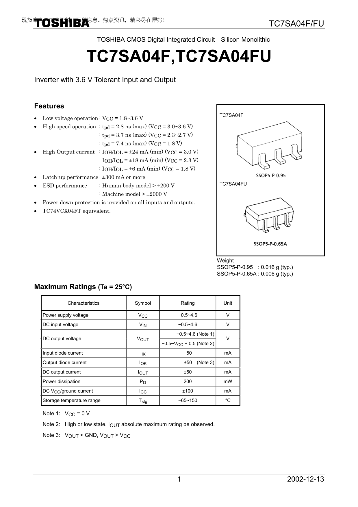
Page 1 Text Content
TC7SA04F/FU
TOSHIBA CMOS Digital Integrated Circuit Silicon Monolithic
TC7SA04F,TC7SA04FU Inverter with 3.6 V Tolerant Input and Output
Features
TC7SA04F
Low voltage operation : VCC = 1.8~3.6 V High speed operation : tpd = 2.8 ns (max) (VCC = 3.0~3.6 V) : tpd = 3.7 ns (max) (VCC = 2.3~2.7 V) : tpd = 7.4 ns (max) (VCC = 1.8 V) High Output current : IOH/IOL = ±24 m A (min) (VCC = 3.0 V) : IOH/IOL = ±18 m A (min) (VCC = 2.3 V) : IOH/IOL = ±6 m A (min) (VCC = 1.8 V) Latch-up performance : ±300 m A or more
TC7SA04FU
ESD performance : Human body model > ±200 V : Machine model > ±2000 V Power down protection is provided on all inputs and outputs. TC74VCX04FT equivalent.
Weight SSOP5-P-0.95 : 0.016 g (typ.) SSOP5-P-0.65A : 0.006 g (typ.)
Maximum Ratings (Ta = 25°C)
Characteristics Symbol Rating Unit
Power supply voltage VCC −0.5~4.6 V DC input voltage VIN −0.5~4.6 V
−0.5~4.6 (Note 1)
DC output voltage VOUT
−0.5~VCC + 0.5 (Note 2)
Input diode current IIK −50 m A Output diode current IOK ±50 (Note 3) m A DC output current IOUT ±50 m A Power dissipation PD 200 m W DC VCC/ground current ICC ±100 m A Storage temperature range Tstg −65~150 °C
Note 1: VCC = 0 V
Note 2: High or low state. IOUT absolute maximum rating be observed.
Note 3: VOUT < GND, VOUT > VCC
Page Summary Contents For Toshiba TOSHIBA CMOS Digital Integrated Circuit Silicon Monolithic TC7SA04F,TC7SA04FU User Manual and Technical Specifications
Manual Details
| Brand | Toshiba |
|---|---|
| Pages | 9 |
| File Size | 181.45 KB |
| Published | July 16, 2026 |
Enter the captcha to get the download link:

Frequently Asked Questions
这种芯片适用于什么类型的电子设备?
该芯片(TOSHIBA产品)可应用于一般电子设备,如计算机、个人设备、办公设备和家用电器等。
如何判断是否需要考虑ESD保护?
TS7SA04FU具有良好的ESD性能,人体模型>±200 V, 机器模型>±2000V。
该芯片的最大工作温度范围是多少?
其操作温度范围为-65°C到150°C的存储温度范围,以及40°C到85°C的操作温度范围。
在不同的电源电压下,输出电流性能如何变化?
最大输出直流电流(I_OH)随供电电压的变化:3.0V时可达±24mA,1.8V时为±6mA。