Texas Instruments CDCLVP110 Low-Voltage 1 to 10LVPECL HSTL with Selectable Input Clock Driver
Summary
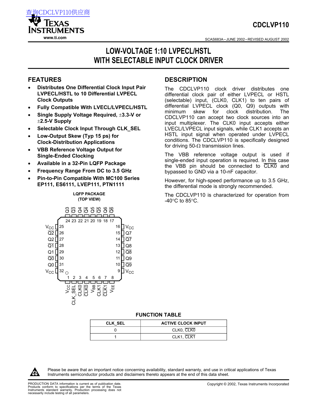
This sophisticated differential clock driver is engineered for high-speed, low-skew clock distribution in critical digital systems. It accepts single or dual LVPECL/HSTL inputs and distributes the signal across ten pairs of complementary outputs, supporting operations up to 3.5 GHz while maintaining compatibility with $50\Omega$ transmission lines. The accompanying technical manual provides comprehensive details on electrical characteristics, pin configurations, supply voltage options, and optimal application guidelines for system designers tackling complex timing requirements.
Page 1 Text Content
查询CDCLVP110供应商
CDCLVP110
www.ti.com
SCAS683A–JUNE 2002–REVISED AUGUST
LOW-VOLTAGE 1:10 LVPECL/HSTL
WITH SELECTABLE INPUT CLOCK DRIVER
LK _S FEATURES LK DESCRIPTION
Distributes One Differential Clock Input Pair
The CDCLVP110 clock driver distributes one
LVPECL/HSTL to Differential LVPECL differential clock pair of either LVPECL or HSTL
Clock Outputs (selectable) input, (CLK0, CLK1) to ten pairs of
LK differential LVPECL clock (Q0, Q9) outputs with•
Fully Compatible With LVECL/LVPECL/HSTL
minimum skew for clock distribution. The•
Single Supply Voltage Required, ±3.3-V or
CDCLVP110 can accept two clock sources into an
±2.5-V Supply
input multiplexer. The CLK0 input accepts either
Selectable Clock Input Through CLK_SEL LVECL/LVPECL input signals, while CLK1 accepts an
HSTL input signal when operated under LVPECL•
Low-Output Skew (Typ ps) for
conditions. The CDCLVP110 is specifically designed Clock-Distribution
Applications
for driving 50-Ω transmission lines.
VBB Reference Voltage Output for
The VBB reference voltage output is used if Single-Ended
Clocking
single-ended input operation is required. In this case•
Available in 32-Pin LQFP Package
the VBB pin should be connected to CLK0 and
Frequency Range From DC to 3.5 GHz bypassed to GND via 10-n F capacitor.
Pin-to-Pin Compatible With MC100 Series
However, for high-speed performance up to 3.5 GHz,
EP111, ES6111, LVEP111, PTN1111
the differential mode is strongly recommended.
LQFP PACKAGE
The CDCLVP110 is characterized for operation from
(TOP VIEW)
-40°C to 85°C.
VCC VCC Q2 Q7 Q2 Q7 Q1 Q8 Q1 Q8 Q0 Q9 Q0 Q9 VCC VCC
FUNCTION TABLE
CLK_SEL ACTIVE CLOCK INPUT
CLK0, CLK0
CLK1, CLK1
Please be aware that an important notice concerning availability, standard warranty, and use in critical applications of Texas
Instruments semiconductor products and disclaimers thereto appears at the end of this data sheet.
PRODUCTION DATA information is current as of publication date. Copyright 2002, Texas Instruments Incorporated
Products conform to specifications per the terms of the Texas
Instruments standard warranty. Production processing does not
necessarily include testing of all parameters.
Page Summary Contents For Texas Instruments CDCLVP110 Low-Voltage 1 to 10LVPECL HSTL with Selectable Input Clock Driver
Manual Details
| Brand | Texas Instruments |
|---|---|
| Pages | 11 |
| File Size | 120.18 KB |
| Published | July 22, 2026 |
Enter the captcha to get the download link:

Frequently Asked Questions
What voltage supply is required for the CDCLVP110?
The device requires a single supply voltage of ±3.3-V or can accept two clock sources into an ±2.5-V Supply input multiplexer.
How do I select between CLK0 and CLK1 input pairs?
Use the CLK_SEL pin: setting it to 0 selects CLK0, and setting it to 1 selects CLK1.
What low-skew copies of the clock are provided?
The outputs Q[9:0] (pins 20, 22, 24, 27) provide LVECL/LVPECL clock outputs with low skew, and pins 29, 31 provide complementary copies.
Is an external reference voltage needed for single-ended operation?
Yes, the VBB pin should be connected to CLK0 and bypassed to GND via a 10-nF capacitor.