Texas Instruments CDC111 1-LINE to 9-LINE Differential LVPECL Clock Driver Data Sheet User Manual
Summary
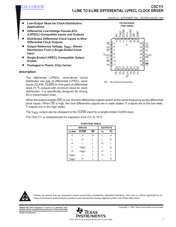
The CDC111 is a professional differential LVPECL clock driver designed to distribute critical 1-line inputs across nine corresponding differential outputs with minimal skew, making it ideal for high-speed, low-skew clock distribution applications. This manual provides comprehensive technical specifications, including electrical characteristics, operating voltage ranges, and absolute maximum ratings. It serves engineers and circuit designers who require reliable, precision timing solutions for driving 50-W transmission lines in demanding digital systems.
Page 1 Text Content
查询CDC111供应商 CDC111
1-LINE TO 9-LINE DIFFERENTIAL LVPECL CLOCK DRIVER
SCAS321G – SEPTEMBER 1993 – REVISED AUGUST 1999
Low-Output Skew for Clock-Distribution FN PACKAGE (TOP VIEW)
Applications Differential Low-Voltage Pseudo-ECL (LVPECL)-Compatible Inputs and Outputs Distributes Differential Clock Inputs to Nine Differential Clock Outputs
Output Reference Voltage, VREF, Allows
Distribution From a Single-Ended Clock
Input
VCC0 VCC0
Single-Ended LVPECL-Compatible Output Y7 Y1 Enable Y6 Y2
Packaged in Plastic Chip Carrier Y6 Y2
description The differential LVPECL clock-driver circuit distributes one pair of differential LVPECL clock
NC – No internal connection
inputs (CLKIN, CLKIN) to nine pairs of differential clock (Y, Y) outputs with minimum skew for clock distribution. It is specifically designed for driving 50-Ω transmission lines. When the output-enable (OE) is low, the nine differential outputs switch at the same frequency as the differential clock inputs. When OE is high, the nine differential outputs are in static states (Y outputs are in the low state, Y outputs are in the high state). The VREF output can be strapped to the CLKIN input for a single-ended CLKIN input. The CDC111 is characterized for operation from 0°C to 70°C.
FUNCTION TABLE LK IN
INPUTS OUTPUTS
LK IN
CLKIN CLKIN OE Yn Yn
VREF VREF
VREF VREF
Please be aware that an important notice concerning availability, standard warranty, and use in critical applications of Texas Instruments semiconductor products and disclaimers thereto appears at the end of this data sheet.
Copyright 1999, Texas Instruments Incorporated PRODUCTION DATA information is current as of publication date.
Products conform to specifications per the terms of Texas Instruments standard warranty. Production processing does not necessarily include testing of all parameters.
1POST OFFICE BOX 655303 • DALLAS, TEXAS 75265
Page Summary Contents For Texas Instruments CDC111 1-LINE to 9-LINE Differential LVPECL Clock Driver Data Sheet User Manual
Manual Details
| Brand | Texas Instruments |
|---|---|
| Pages | 7 |
| File Size | 95.55 KB |
| Published | June 17, 2026 |
Enter the captcha to get the download link:

Frequently Asked Questions
What is the input compatibility of the CDC111?
It has differential low-voltage pseudo-ECL (LVPECL)-compatible inputs and outputs.
What is the operating temperature range for the CDC111?
The CDC111 is characterized for operation from 0°C to 70°C.
What happens when the output-enable (OE) is high?
The nine differential outputs are in static states: Y outputs are low, Y outputs are high.
What is the recommended supply voltage range?
The recommended supply voltage range is 3 V to 3.6 V.