Texas Instruments CD74AC238 3-LINE TO 8-LINE DECODER/DEMULTIPLEXER datasheet manual
Summary
This technical guide details the high-performance CD74AC238 decoder/demultiplexer, an essential component for advanced memory decoding and data routing applications. Designed for efficient operation in systems requiring ultra-low propagation delays, it utilizes a 3-to-8 line decoding architecture. The manual provides comprehensive specifications, including voltage ranges (1.5V–5.5V), output drive capabilities, and simple enable input solutions for easy system expansion. It is ideal for electrical engineers building high-speed digital logic circuits and complex data management systems.
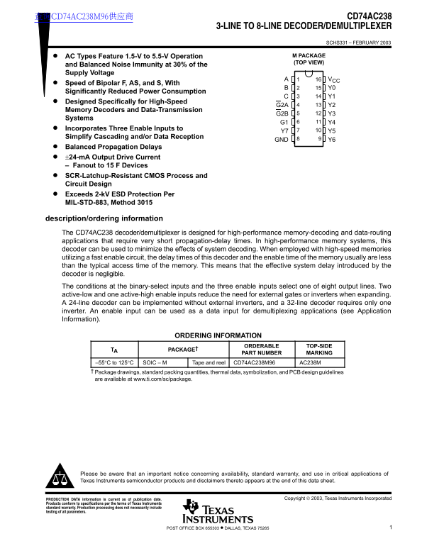
Page 1 Text Content
查询CD74AC238M96供应商 CD74AC238
3-LINE TO 8-LINE DECODER/DEMULTIPLEXER
SCHS331 – FEBRUARY 2003
AC Types Feature 1.5-V to 5.5-V Operation M PACKAGE (TOP VIEW)
and Balanced Noise Immunity at 30% of the Supply Voltage
Speed of Bipolar F, AS, and S, With
Significantly Reduced Power Consumption
Designed Specifically for High-Speed
Memory Decoders and Data-Transmission
Systems
Incorporates Three Enable Inputs to
Simplify Cascading and/or Data Reception
GND Y6
Balanced Propagation Delays ±24-m A Output Drive Current – Fanout to 15 F Devices SCR-Latchup-Resistant CMOS Process and Circuit Design Exceeds 2-k V ESD Protection Per MIL-STD-883, Method 3015
description/ordering information The CD74AC238 decoder/demultiplexer is designed for high-performance memory-decoding and data-routing applications that require very short propagation-delay times. In high-performance memory systems, this decoder can be used to minimize the effects of system decoding. When employed with high-speed memories utilizing a fast enable circuit, the delay times of this decoder and the enable time of the memory usually are less than the typical access time of the memory. This means that the effective system delay introduced by the decoder is negligible. The conditions at the binary-select inputs and the three enable inputs select one of eight output lines. Two active-low and one active-high enable inputs reduce the need for external gates or inverters when expanding. A 24-line decoder can be implemented without external inverters, and a 32-line decoder requires only one inverter. An enable input can be used as a data input for demultiplexing applications (see Application Information).
ORDERING INFORMATION
ORDERABLE TOP-SIDE
TA PACKAGE†
PART NUMBER MARKING
–55°C to 125°C SOIC – M Tape and reel CD74AC238M96 AC238M Package drawings, standard packing quantities, thermal data, symbolization, and PCB design guidelines are available at www.ti.com/sc/package.
Please be aware that an important notice concerning availability, standard warranty, and use in critical applications of Texas Instruments semiconductor products and disclaimers thereto appears at the end of this data sheet.
Copyright 2003, Texas Instruments Incorporated PRODUCTION DATA information is current as of publication date.
Products conform to specifications per the terms of Texas Instruments standard warranty. Production processing does not necessarily include testing of all parameters.
1POST OFFICE BOX 655303 • DALLAS, TEXAS 75265
Page Summary Contents For Texas Instruments CD74AC238 3-LINE TO 8-LINE DECODER/DEMULTIPLEXER datasheet manual
Manual Details
| Brand | Texas Instruments |
|---|---|
| Pages | 11 |
| File Size | 212.05 KB |
| Published | June 05, 2026 |
Enter the captcha to get the download link:

Frequently Asked Questions
What is the primary function and benefit of this decoder in high-speed memory systems?
It functions as a 3-line (G1, G2A, G2B) to 8-line decoder/demultiplexer, designed to keep system decoding delay negligible compared to typical memory access time.
How can the device be used in demultiplexing applications?
An enable input (C, B, or A) can be utilized as a data input for general demultiplexing purposes.
What are the specified electrical limits and output capabilities?
The supply voltage ranges from -0.5 V to 6 V CC, with a continuous output current of up to ±50 mA per pin.
Does this device incorporate features for reliability in demanding environments?
Yes; it includes an SCR-Latchup-Resistant CMOS Process and Exceeds 2-kV ESD protection according to MIL-STD-883, Method 3015.