Texas Instruments SN54AHC139, SN74AHC139 Dual 2-Line to 4-Line Decoders/Demultiplexers Data Manual/Owner's Manual
Summary
This dual 2-line to 4-line decoder/demultiplexer (SN54AHC139) is engineered for high-speed memory decoding and critical data routing applications. It operates across a voltage range of 2V to 5.5V, minimizing system delay in demanding electronic systems. The accompanying technical manual details comprehensive performance specifications, packaging options, advanced electrical ratings, and functional guidelines necessary for engineers developing reliable, efficient digital circuits.
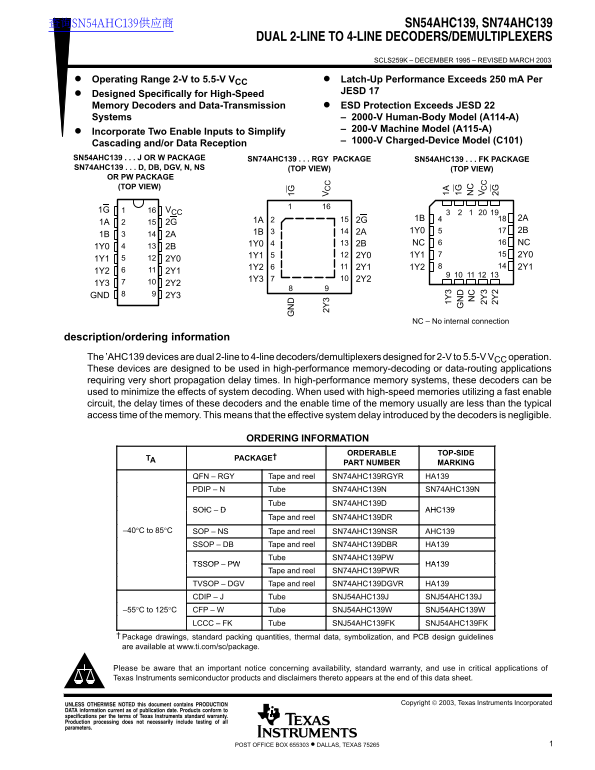
Page 1 Text Content
查询SN54AHC139供应商 SN54AHC139, SN74AHC139
DUAL 2-LINE TO 4-LINE DECODERS/DEMULTIPLEXERS
SCLS259K – DECEMBER 1995 – REVISED MARCH 2003
Operating Range 2-V to 5.5-V VCC Latch-Up Performance Exceeds 250 m A Per
JESD 17
Designed Specifically for High-Speed Memory Decoders and Data-Transmission ESD Protection Exceeds JESD 22 Systems – 2000-V Human-Body Model (A114-A)
– 200-V Machine Model (A115-A)
Incorporate Two Enable Inputs to Simplify
– 1000-V Charged-Device Model (C101)
Cascading and/or Data Reception SN54AHC139 J OR W PACKAGE SN74AHC139 RGY PACKAGE SN54AHC139 FK PACKAGE SN74AHC139 D, DB, DGV, N, NS (TOP VIEW) (TOP VIEW) OR PW PACKAGE (TOP VIEW)
1G VCC
1Y0 2B NC NC
GND 2Y3
NC – No internal connection
description/ordering information The ’AHC139 devices are dual 2-line to 4-line decoders/demultiplexers designed for 2-V to 5.5-V VCC operation. These devices are designed to be used in high-performance memory-decoding or data-routing applications requiring very short propagation delay times. In high-performance memory systems, these decoders can be used to minimize the effects of system decoding. When used with high-speed memories utilizing a fast enable circuit, the delay times of these decoders and the enable time of the memory usually are less than the typical access time of the memory. This means that the effective system delay introduced by the decoders is negligible.
ORDERING INFORMATION
ORDERABLE TOP-SIDE
TA PACKAGE† 1G
PART NUMBER MARKING
QFN – RGY Tape and reel SN74AHC139RGYR HA139
PDIP – N Tube SN74AHC139N SN74AHC139N
Tube SN74AHC139D
SOIC AHC139
Tape and reel SN74AHC139DR
–40°C to 85°C SOP – NS Tape and reel SN74AHC139NSR AHC139
SSOP – DB Tape and reel SN74AHC139DBR HA139
Tube SN74AHC139PW
TSSOP PW HA139 –
Tape and reel SN74AHC139PWR
TVSOP – DGV Tape and reel SN74AHC139DGVR HA139 CDIP – J Tube SNJ54AHC139J SNJ54AHC139J
–55°C to 125°C CFP – W Tube SNJ54AHC139W SNJ54AHC139W
LCCC – FK Tube SNJ54AHC139FK SNJ54AHC139FK
Package drawings, standard packing quantities, thermal data, symbolization, and PCB design guidelines are available at www.ti.com/sc/package.
Please be aware that an important notice concerning availability, standard warranty, and use in critical applications of Texas Instruments semiconductor products and disclaimers thereto appears at the end of this data sheet.
Copyright 2003, Texas Instruments Incorporated UNLESS OTHERWISE NOTED this document contains PRODUCTION
DATA information current as of publication date. Products conform to specifications per the terms of Texas Instruments standard warranty. Production processing does not necessarily include testing of all parameters.
1POST OFFICE BOX 655303 • DALLAS, TEXAS 75265
Page Summary Contents For Texas Instruments SN54AHC139, SN74AHC139 Dual 2-Line to 4-Line Decoders/Demultiplexers Data Manual/Owner's Manual
Manual Details
| Brand | Texas Instruments |
|---|---|
| Pages | 14 |
| File Size | 479.48 KB |
| Published | June 18, 2026 |
Enter the captcha to get the download link:

Frequently Asked Questions
What is the primary function of this semiconductor device?
It acts as a dual 2-line to 4-line decoder/demultiplexer.
Is this device suitable for high-speed memory applications?
Yes, it is designed for high-performance decoding and data routing where delays are negligible.
What is the specified supply voltage operating range?
The operational supply voltage range is –0.5V to 7V.
How can the enable input (G) be utilized in demultiplexing?
The active-low enable (G) input can also function as a data line in demultiplexing applications.