# A B C D E F G H I J K L M N O P Q R S T U V W X Y Z

ST TL074 Low noise JFET quad operational amplifier Data Handbook

Summary

The TL074 is a high-performance quad operational amplifier featuring JFET inputs for superior circuit stability and low noise. Known for its high slew rate, minimal bias/offset currents, and wide common-mode voltage range, it excels in demanding analog signal processing applications. This detailed datasheet provides electrical characteristics, maximum ratings, and comprehensive operating guidelines necessary for engineers designing reliable and accurate circuits.
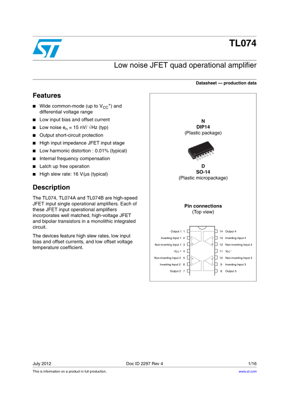
📄 Preview 📖 Table of Contents Contents PAGE OF 16

Page 1 Text Content

TL074

Low noise JFET quad operational amplifier

Datasheet — production data

Features

+) and

Wide common-mode (up to VCC differential voltage range Low input bias and offset current

Low noise en = 15 n V/ √Hz (typ) DIP14 (Plastic package)

Output short-circuit protection High input impedance JFET input stage Low harmonic distortion : 0.01% (typical) Internal frequency compensation Latch up free operation

SO-14

High slew rate: 16 V/µs (typical)

(Plastic micropackage)

Description The TL074, TL074A and TL074B are high-speed JFET input single operational amplifiers. Each of

Pin connections

these JFET input operational amplifiers

(Top view)

incorporates well matched, high-voltage JFET and bipolar transistors in a monolithic integrated circuit.

Output 1 Output 4

The devices feature high slew rates, low input

Inverting Input 1 Inverting Input 4

bias and offset currents, and low offset voltage

Non-inverting Input 1 Non-inverting Input 4

temperature coefficient.

CCV -CCV

Non-inverting Input 2 Non-inverting Input 3

Inverting Input 2 Inverting Input 3

Output 2 Output 3

July 2012 Doc ID 2297 Rev 4 1/16 This is information on a product in full production. www.st.com

Page Summary Contents For ST TL074 Low noise JFET quad operational amplifier Data Handbook

Page 1 TL074 Low noise JFET quad operational amplifier Datasheet — production data Features +) and Wide common-mode (up to VCC differential voltage range Low input bias and offset current Low noise en = 15 n...
Page 2 Schematic diagram TL074 1 Schematic diagram Figure 1. Circuit schematics Non- inver ting input Inverting input Output Ω1 1/4 TL074 2/16 Doc ID 2297 Rev 4
Page 3 TL074 Absolute maximum ratings and operating conditions 2 Absolute maximum ratings and operating conditions Table 1. Absolute maximum ratings Value Symbol Parameter Unit TL074I, AI, BI TL074C, AC, BC ...
Page 4 Electrical characteristics TL074 3 Electrical characteristics Table 3. VCC = ±15V, Tamb = +25°C (unless otherwise specified) TL074I,AC,AI, BC,BI TL074C Symbol Parameter Unit Min. Typ. Max. Min. Typ. M...
Page 5 TL074 Electrical characteristics Table 3. VCC = ±15V, Tamb = +25°C (unless otherwise specified) (continued) TL074I,AC,AI, BC,BI TL074C Symbol Parameter Unit Min. Typ. Max. Min. Typ. Max. Rise time tr ...
Page 6 Electrical characteristics TL074 Figure 2. Maximum peak-to-peak output Figure 3. Maximum peak-to-peak output voltage versus frequency voltage versus frequency Figure 4. Maximum peak-to-peak output Fig...
Page 7 TL074 Electrical characteristics SU PP LY UR EN (m A) IN PU BI AS EN (n A) Figure 8. Input bias current versus free air Figure 9. Large signal differential voltage temperature amplification versus fre...
Page 8 Electrical characteristics TL074 EQ IV AL EN IN PU NO IS VO LT AG (n V/ VH z) Figure 14. Voltage follower large signal pulse Figure 15. Output voltage versus elapsed time response OVERSHOOT = 15V CC 1...
Page 9 TL074 Parameter measurement information 4 Parameter measurement information Figure 18. Voltage follower Figure 19. Gain-of-10 inverting amplifier TL074 RL CL= 100p F Doc ID 2297 Rev 4 9/16
Page 10 Typical applications TL074 5 Typical applications Figure 20. Audio distribution amplifier f = 100k Hz O Output A TL074 1μF TL074 Output B Input TL074 1OO μF Output C TL074 Figure 21. Positive feeback ...
Page 11 TL074 Typical applications Figure 22. Output A Figure 23. Output B SECOND ORDER BANDPASS FILTER CASCADED BANDPASS FILTER fo = 100 k Hz; Q = 30; Gain = 16 fo = 100 k Hz; Q = 69; Gain = 16 Doc ID 2297 R...
Page 12 Package information TL074 6 Package information In order to meet environmental requirements, ST offers these devices in different grades of ECOPACK® packages, depending on their level of environmental...
Page 13 TL074 Package information 6.2 SO-14 package information Figure 25. SO-14 package mechanical drawing Doc ID 2297 Rev 4 13/16
Page 14 Package information TL074 Table 5. SO-14 mechanical data Min. Typ. Max. ddd 0.10 14/16 Doc ID 2297 Rev 4
Page 15 TL074 Ordering information 7 Ordering information Table 6. Order codes Temperature Order code Package Packing Marking range TL074IN TL074IN TL074AIN DIP14 Tube TL074AIN TL074BIN TL074BIN TL074ID/IDT 0...
Page 16 TL074 Please Read Carefully: Information in this document is provided solely in connection with ST products. STMicroelectronics NV and its subsidiaries (“ST”) reserve the right to make changes, correc...

Manual Details

Brand QUAD
Pages 16
File Size 320.85 KB
Published June 04, 2026
44 views

Enter the captcha to get the download link:

captcha

Frequently Asked Questions

What is the optimal operating temperature range?

The typical operational free-air temperature ranges are -40 to +105 °C for DIP14 and 0 to +70 °C for SO-14.

Does the amplifier offer short-circuit protection?

Yes, the devices feature output short-circuit protection.

What is the maximum input voltage allowed relative to supply?

The non-inverting input voltage must never exceed the magnitude of the supply voltage or 15 volts, whichever is less.

How low can the amplifier's noise be?

It has a low typical noise value of 15 nV/√Hz (for plastic package).

What kind of packages are available for this chip?

The TL074 is available in DIP14 and SO-14 packages, among others.